
I often get questions from my fellow design engineers from around the world asking why we should or should not use S parameters or Z parameters for power distribution network (PDN) designs or validation. The truth is, we should be familiar with both, because depending on our design and validation tools, one or the other may be better suited for the task.
The timeliness of this question is underlined by the fact that as I am finishing up this manuscript, an article on a similar topic just appeared in Printed Circuit Design &Fab Magazine [1]. To get the answer, first we need to understand the task on hand and the circumstances that eventually may guide us toward one or the other choice.
We have to start stating that all this discussion assumes that we look at the response of a linear and time invariant system. If these assumptions are true, mathematically speaking it does not matter which network-matrix representation we chose to use. The decision depends on practical details, which of course, will depend on the actual circumstances.
To its mathematical precision, none of our physical circuits may meet these stringent requirements. On the other hand, for our practical purposes, it is enough if our system is linear and time invariant to a degree that the effects of nonlinearity and/or time variance can be neglected in the result. For instance, a lot of high-density ceramic multi-layer capacitors that we use today in our PDNs exhibit DC and AC bias dependencies, which are manifestations of minor nonlinear behavior. To illustrate this, in Fig. 1 we reproduce data from [2].
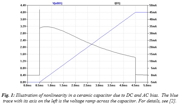
This nonlinearity is noticeable, but for almost all of our PDN applications, we can ignore it as long as the fluctuation of voltage across the capacitor is small. This does not mean that we ignore the effect of DC bias sensitivity altogether; it means that we linearize the behavior around the DC operating point.
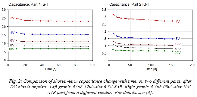
We can also catch time variance that may arise due to multiple causes. For instance, staying with Class-II ceramic capacitors, we can witness time dependency in the aging process, which is usually slow enough that we can ignore the change during the time-window of our simulations and use the average value at any given point in time along the slow aging process. In addition to long-term aging, in some parts we may also see short-term relaxation effects after applying the DC bias voltage. As an illustration, on two different ceramic capacitors, Fig. 2 shows measured data showing capacitance change due to short-term relaxation.
Another situation when change of circuit behavior over time may become noticeable is thermal drift in power circuits. The circuit may change as the components heat up or cool down according to their actual workload (or due to changes in ambient temperature). This can happen in high-density DC-DC converters where the impact of thermal excursion may noticeably change the losses of power components and control-loop behavior. It can corrupt a low-frequency sweep that could last several seconds, sometimes minutes.
With the above introduction, once we convince ourselves that nonlinearities and time variance can be, in fact, ignored, we are left with the black-box equivalent circuit in Fig. 3. For the sake of simplicity, here we show a four-port circuit, but the number of ports can be any positive integer. Each port has two terminals and we mark the voltages and currents at each port.
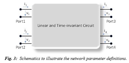
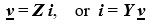
We can relate the voltages and currents through a number of different ways, leading to the various matrix representations of the coefficients. For instance, if we combine all terminal voltages into a v vector and all currents into an i vector, the connection between them is the impedance matrix or admittance matrix, dependent on which vector contains the independent or dependent variables.
In the early days of electronic designs and calculations, impedance and admittance were commonly used. They offer very convenient ways to characterize low and medium-frequency circuits and the conditions to identify matrix elements are a good match for our common-sense practices.
The impedance matrix is very convenient when it comes to measurement: the condition to measure impedance between any two ports is to connect a current source to one of the two ports and measure the resulting voltage at the other port (which, in case of self impedance, can be the same single port). All other ports can (and should be) left open, which is a huge convenience.
It is also a significant convenience that we can add and drop ports at any time without having to change or redo anything else. For instance, if we measure or simulate the impedance between Port 1 and Port 2, the Z21 and (in case of a reciprocal system the identical) Z12 values will remain valid if we add new ports or delete any of the other ports.
We also know that in the PDN design process, when we do it in the frequency domain, impedance is preferred and used. This comes from the fact that usually the PDN noise sources and loads have much higher impedance than the PDN network itself, so the noise sources can be approximated by current sources. When we calculate the noise voltage at the load from the excitation current, the two are connected by impedance.
At higher frequencies, however, leaving a circuit port open does not equate to infinite impedance: the fringing field creates an increasing error at higher frequencies. The fringing fields at the ports can be contained if we put shorts on the ports: this leads us to the admittance matrix, which calculates a matrix element by applying voltage at the source port and measure the current through the short at the destination port, while all other ports are shorted.
Connecting shorts to the ports will extend the usable frequency range in measurements, but it comes with the inconvenience of needing to put shorts on all ports, not just the ones we actually look at. This also means that if we add or drop ports, measurements or simulations have to be recalculated with the new port assignment. In computations, on the other hand, the admittance matrix is the favorite, partly because open (infinite impedance) translates to zero admittance, which creates less numerical problem than shorts, which would translate to infinite admittance, potentially causing numerical issues.
As we move to even higher frequencies, we will notice that positioning the shorts is becoming more critical and eventually the short ‘loses its effectiveness.’ This happens when the wavelength of the test signal is no longer negligible compared to the distances in our system.
So, unless we can position the physical short (which, in itself, will also be less than ideal at high frequencies) exactly where we think it should be, we will end up with an impedance from the short transformed through the misalignment distance of the interconnect. When this happens, we need to turn to describing our system with waves, rather than simply voltages and currents.
Voltages and currents still apply, but now we have to consider the fact that the current, flowing in loops, will describe signals (waves) potentially traveling in opposite directions. Eventually the matrix of scattering parameters is defined as [4]
b = S a
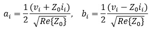
where the a and b vectors are the collections of incident and reflected waves, respectively, at the ports. The waves combine voltages and currents such that they represent the direction of the wave. For identical Z0 characteristic impedance on all ports, the incident and reflected waves can be expressed with the voltages and currents as
The great benefit of the scattering matrix is that instead of open or short, all ports need to be terminated with their Z0 characteristic impedance, which is much less sensitive to precise positioning than an extreme termination. The price we have to pay for this convenience is that here, too, adding or dropping ports, either in simulations or in measurements, will require a recalculation or remeasuring the matrix, just as when we use the admittance matrix.
Reciprocal systems will have symmetric scattering matrices, namely the matrix elements are symmetric along the main diagonal. For a two-port circuit, this translates to S21 = S12. When a circuit shows electrical symmetry, it will translate to symmetry of the scattering matrix along the off diagonal. For a symmetric two port circuit, it means that S11 = S22. As a result, our typical uniform interconnects, such as a uniform PCB trace or cable, can be described with just two matrix elements: a reflection and a transmission element.
As we argue above, we use a scattering matrix to overcome measurement difficulties at higher frequencies. As it was shown in earlier works, due to practical limitations of how our instruments work, to measure a low-impedance PDN circuit, we need to measure the impedance with two-port shunt-through connections [5], and we should use the transmission results and ignore the reflection results.
If the instruments were ideal, we could just use a one-port reflection measurement and calculate the impedance from the reflection, or we could back-calculate the unknown impedance also from the reflection of the two-port shunt-through scattering data and we would get exactly the same result. For two-port models, this was illustrated in [6] with accurate S-parameter models from the Murata SimSurf tool [7].
Fig. 4 shows the four plots of the S-parameter magnitudes for all four matrix elements for a ceramic capacitor modeled in the two-port shunt mode. As [6] explained, though the model is based on measured data, this is not directly the measurement data. The measured data also contains measurement noise and errors due to minor imperfections. Instead, the model is a causal and passive fitted model on the measured data. As a result, we get the ideal symmetry and reciprocity (S11 = S22 and S21 = S12), moreover—as opposed to when we have measured data—both the reflection and transmission terms are accurate enough to calculate the impedance.
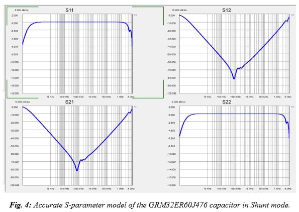
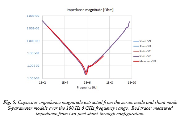
Fig. 5 shows this: the impedance of the capacitor can be accurately reconstructed from either the reflection or the transmission term from either the shunt-through or the series-through model. Note that the series-through model is convenient for measuring high impedances, namely low-valued capacitors.
You may also wonder why do we show two-port (four-terminal) S-parameter models for capacitors, which usually have just two terminals? The reason is: that is what we currently get from vendors. If we check the websites of leading capacitor vendors (I recently checked Murata, TDK, Taiyo-Yuden, Kemet, Yageo, Panasonic), we see that their S-parameter models are all two-port models. They do not offer Z-parameter models, but two-terminal SPICE equivalent circuits are readily available.
From most vendors, S-parameter models are available for one configuration only (either two-port shunt-through or two-port series-through); from Murata, models are available for both configurations. Popular simulators will take any of these models, but you need to pay attention to how the simulator interprets the two-port capacitor models, because not all simulators will automatically detect the series or shunt nature of the model.
There is one new element though in the scattering matrix that we also have to pay attention to: the Z0 reference impedance. In signal integrity, when we use transfer parameters, we are usually interested in the propagation of our high-speed signals. We want to see the attenuation and delay of a channel as a function of frequency between matched (or almost matched) terminations.
For multiple reasons, the sweet spot for interconnect and instrumentation impedance is in a relatively narrow range around 50 ohms, and it serves us quite well for signal-integrity purposes, even if the actual single-ended system impedance is somewhat different. PDN impedances, on the other hand, are markedly different. PDN impedance may be hundreds of ohms for very low power circuits and may be sub-milliohm for very high-power circuits, and anything in between. So, selecting a ‘typical’ reference impedance is not really practical, also because often we need to measure PDN components or circuits where the impedance varies orders of magnitudes within the measurement frequency range. As an example, the impedance magnitude in Fig. 5 varies in a 10,000:1 range.
For measurements, we cannot easily choose or change our reference impedance. Certainly, the measuring instrument and its immediate cabling have their given characteristic impedance, usually 50 Ohm. Changing that impedance orders of magnitudes up or down is not practical. If we need to, we can change the reference impedance very close to the DUT, where no further cabling is needed to reach the DUT, see [8] for details.
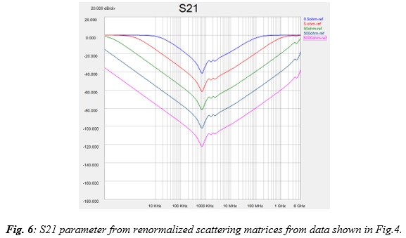
The numerical dynamic range of CAD tools is much larger than the dynamic range of measuring instruments, and therefore we can renormalize the scattering matrix for a different reference impedance in a wide range. Fig. 6 illustrates that with a commercial tool (here I used [9]) we can change the reference impedance in a 10,000:1 (80 dB) range with no problem.
We see that when we plot the scattering parameters with different normalization impedances, we get the proportional vertical shift and the corresponding saturation near 0 dB, but if we calculate the impedance from any of these renormalized scattering matrices, we get exactly the original impedance profile we have in Fig. 5. This being said, when we simulate very complex low-impedance circuits requiring a lot of matrix manipulations to give us the final result, people found that it is a good idea to help the simulator by moving the reference impedance into the vicinity of the impedance of our structure. 0.1 Ohms has been a typical reference impedance in such cases.
In summary, we showed that for bypass capacitors, other than SPICE equivalent circuit models, only S-parameter simulation models are available from vendors. Also, due to practical limitations, measurements of low-impedance PDN circuits are typically performed with scattering matrices, though direct impedance measurement based on current and voltage ratios is also doable. In the frequency-domain power distribution design and validation processes, we start and finish with impedance, but along the way simulations and measurements often use S parameters. So it is best if we are familiar with both.
References:
[1] “You Don’t Always Need S-parameters,” Printed Circuit Design & Fab / Circuits Assembly, November 2020.
[2] “Dynamic Models for Passive Components,” http://www.electrical-integrity.com/Quietpower_files/QuietPower-36.pdf
[3] “DC and AC Bias Dependence of Capacitors,” DesignCon 2011
[4] Scattering parameters, https://en.wikipedia.org/wiki/Scattering_parameters
[5] “Measuring milliohms and Picohenrys,” DesignCon 2000.
[6] “What You Need to Know About Bypass Capacitor S-Parameter Models,” http://www.electrical-integrity.com/Quietpower_files/QuietPower-51.pdf
[7] Murata SimSurfing tool, https://ds.murata.co.jp/simsurfing/index.html?lcid=en-us
[8] https://ieeexplore.ieee.org/document/7851286/
[9] N1930B Physical Layer Test System (PLTS) 2020 Software, https://www.keysight.com/