
If you’ve been working on PCB designs most of your career, and you have experience with layout and routing for computer interfaces, then you know one thing to be true: take recommendations in component application notes with a grain of salt. It’s not that these notes are always wrong, but the recommendations can be easily taken out of context.
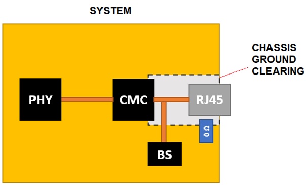
One recommendation that was pointed out to me by a colleague regards the use of a ground plane below RJ45 connectors when routing between discrete magnetics and the connector. Some application notes recommend running the system ground plane right up to the RJ45 connector, and some application notes recommend splitting the ground plane into system and chassis portions to provide stronger isolation. Some recommendations in application notes state that the ground plane should be omitted entirely from beneath the PHY, magnetics, and/or the RJ45 jack.
So which is correct? The designers I work with, and recent boards we worked on, always include a system plane with chassis cutout up to the edge of the RJ45, even when multiple connectors are placed in parallel. As I looked through different recommendations on forums, other professional designers claim they’ve never had a problem removing all ground plane regions between the output side of the common-mode choke and the RJ45. Let’s dig into this a bit deeper and see if we can understand where these differences arise, and when it is appropriate to have a continuous plane, split planes, or no planes under an RJ45 connector.
Ethernet Layout and the Function of Ground Planes
To look more at this idea of ground planes beneath different portions of an Ethernet system and connector, let’s briefly look at the routing requirements for Ethernet and RJ45 connectors. An Ethernet system consists of a MAC/PHY interface (usually integrated into a single IC), a magnetics circuit for common-mode noise suppression and termination, other passives for termination (usually pull-up or Thevenin termination), and the RJ45 connector. Rx and Tx lines are routed in parallel throughout the system. The number, values, and arrangement of passives depends on the exact routing standard (e.g., Base-T vs. power over Ethernet) and PHY interface.
Traces between the MAC/PHY, magnetics circuit, and the RJ45 connector are routed as differential pairs with defined impedance. Note that this includes traces within a discrete magnetics circuit. The differential impedance is set to 100 Ohms to provide matching to the cable’s differential impedance. Shorter traces are generally preferred throughout, especially at higher frequencies (e.g., gigabit Ethernet and higher) to reduce losses. Everyone who works with Ethernet is pretty clear on these requirements.
The controversy around the ground plane (or planes) starts with placement of discrete magnetics and any other components needed for termination with respect to the PHY and RJ45 connector. There are generally three possibilities:
Option 1: Run the system ground up to the RJ45 connector, regardless of whether magnetics are integrated into the connector; or
Option 2: Use a split ground plane, where chassis ground is placed below the RJ45 and system ground runs to the input edge of the common-mode choke; or
Option 3: Place no ground plane between the magnetics input and the RJ45 connector.
The answer to this question relies on a few points: how random displacement currents (noise) in a ground plane behave near the common-mode choke, whether the magnetics are integrated into the connector, and whether chassis grounding is needed between the magnetics and RJ45 to ensure EMI protection and isolation.
Before we look at which of these options is objectively best for routing between a PHY, magnetics, and the RJ45 connector, it helps to review the overall design goals:
Design Goal 1: ESD/overvoltage protection. The 802.3 standard specifies the Ethernet PHY must be isolated from the rest of the system in order to withstand high-potential AC up to 1500 V(RMS) at 50 to 60 Hz for 60 seconds.
Design Goal 2: noise isolation. Any noise picked up on the cable should be prevented from coupling back into the PHY and rest of the board.
Design Goal 3: common-mode noise shunt. Common-mode noise in any ground region should be diverted away from the magnetics and PHY side through low impedance paths.
All of these design goals might be addressed in different ways with Options 1-3. The arrangement/coupling of multiple ground planes, or the use of a single continuous ground plane, would determine the level of isolation, ESD protection, and impedance seen by propagating noise currents. To better understand Options 1-3, let’s look at how grounding needs to be arranged for RJ45 connectors with discrete and integrated magnetics.
Integrated vs. Discrete Magnetics
The image below (Figure 1) shows an example schematic for 100 Mbps Ethernet with a typical pull-up resistor scheme near the PHY for termination and shunted connection for common-mode noise at the transformer’s center tap.1 This schematic is intended to show placement of ground regions for discrete magnetics, but it could also apply to RJ45 connectors with integrated magnetics.
The distance between the output of the PHY and the magnetics input should be at least 25 mm. The intention here is to provide sufficient isolation between the magnetics and the PHY, although making these lines too long leads to greater attenuation, and this attenuation is greater at higher frequencies. In both types of connectors, common-mode capacitors can also be placed on the end taps as a shunt to the system ground at the magnetics input to provide greater high frequency noise rejection.
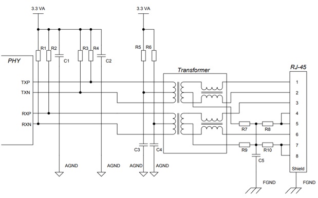
The image above shows a shielded RJ45 connector, where the shielding is connected to the chassis ground alongside the Bob Smith termination resistors. If we have an unshielded RJ45, there is no chassis ground connection from the connector shroud. Note that STP cable needs to be used with a shielded RJ45 connector, but UTP cable could be used with either shielded or unshielded RJ45 connectors. Using a shielded connector on an unshielded cable will yield no benefit in terms of suppressing EMI received in the cable, but it won't cause problems either in practical Ethernet systems.
Gigabit Ethernet and faster will use a similar scheme with four differential pairs and common-mode chokes in the magnetics. Bob Smith termination is almost always used for the center taps on the output side of the magnetics transformer. Some have suggested the Bob Smith termination scheme is not the best option, and lower return loss can be achieved with a different termination scheme.2 I won’t address this issue here as it is deep enough to warrant its own article.
For RJ45 connectors with integrated magnetics, the system ground plane should run to the edge of the connector to provide continuous impedance for the differential lines leading into the connector. The system plane should also run up to the discrete magnetics; this is consistent with the recommendations in.1 In both types of connectors, and if the connector is shielded, the connector shielding is then connected to the chassis ground for ESD protection and to provide shielding from high frequency noise. This is useful in industrial settings where equipment may be present near high voltage sources or near radio equipment.
Many application notes I’ve seen state that the region below the magnetics should not be filled with a ground plane. This leaves the final unanswered question and source of contention in Ethernet routing: do we extend a ground region (system and/or chassis) between the magnetics output and the RJ45?
Chassis and System Ground Layout
Option 1
Visualizing Option 1 is rather simple: just run the system ground plane throughout the 2nd layer. The system ground will run beneath the magnetics and extend up to the RJ45 connector. A shielded connector will sit against the chassis and enclosure, so its internal shielding will be referenced back to the system ground.

The objection to Option 1 is that noise currents in the connector region of the system ground plane can couple common-mode noise back to the PHY side via coupling into the magnetics components (Design Goals 2 and 3). The other objection here relates to Design Goal 1: the Ethernet PHY is supposed to be electrically isolated from the rest of the system under the 802.3 standard, and the ground plane provides a low impedance path for an ESD pulse to reach the PHY and other components. Providing a low impedance return path back to the chassis and eventually the power supply return point still provides ESD protection and a sink for noise.
Ideally, you want noise currents to follow a directed path back to ground, rather than coupling through the isolation barrier. Common-mode noise that couples from the ground plane back to the magnetics and into the PHY side of the system plane will do so capacitively or inductively. Ideally, the magnetics components should have low leakage inductance and low leakage capacitance/parasitic capacitance back to the ground plane. For lower speed Ethernet, leakage inductance will dominate noise transfer as the carrier frequency is lower. In contrast, capacitive parasitics will dominate at higher Ethernet speeds because the carrier frequency is higher.
To satisfy all three design goals with Option 1, this requires the combined system plane to be tied with very low impedance to the chassis. In my opinion, this approach works best with integrated shielded RJ45 connectors as an ESD pulse or noise can be shunted immediately back to the chassis. However, a direct connection to a shielded RJ45 is not required; one would expect an unshielded RJ45 connector to work fine as long as there is a low impedance tie to the chassis.
Note that the continuous ground plane can cause an EMI problem in the form of interference between digital and analog sections if return paths are not planned out properly. In addition, connecting multiple points on the plane back to the chassis can allow currents to form a loop through the chassis, creating a potentially large radiator when there is strong ground bounce potential between the system plane and the chassis.3

Here, you have two separate ground portions: the system ground and a plane region in the PCB that connects to the chassis ground. How do you ensure they remain at the same potential? The chassis ground region should be connected to the other grounds to eliminate potential differences between these regions. This can be done via a low impedance path; something as simple as mechanically fixing the system plane to the chassis or using a 0 Ohm resistor between the chassis and system ground regions is sufficient. Placing a high voltage capacitor is another strategy for bridging the two planes while directing high frequency noise away from the magnetics. The problem with this is that you risk creating a large loop inductance return path between the two sections if not designed properly.
A variation on Figure 3 is to simply use a continuous ground plane with a large hole cut out for the common-mode choke. Don’t do this: you’ve created a large ring of conductor that can receive EMI and induce common-mode noise within a critical region of the system, i.e., after the common-mode choke. You’ve basically cut your total common mode rejection ratio (CMRR) in half.
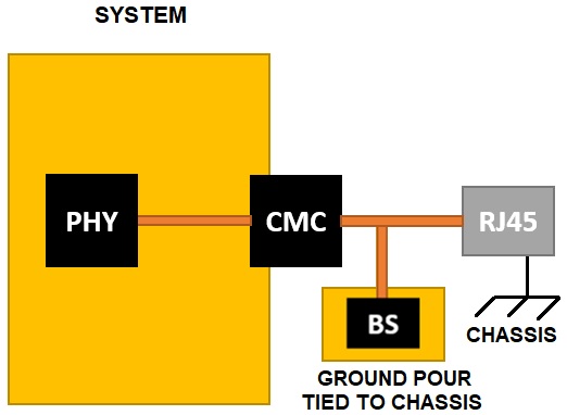
Another variation on Option 2 is shown in Figure 4. This involves placing a ground cutout in the system ground plane that runs up to the board edge, and then placing a chassis layer below the RJ45 connector. The Bob Smith termination network is then placed off to the side and connects back to the system plane. The two plane sections can be set to the same DC potential with a 0 Ohm resistor or internal vias. The RJ45 connector shroud can then be referenced directly back to the chassis ground plane.
The chassis is then connected with a low impedance path back to the system ground. I’ve seen application notes that state a 0 Ohm resistor should be used, while others recommend a capacitor (see [4]). The best connection from an ESD standpoint is to tie them mechanically back to the chassis. Again, we have the same potential for ground currents to exist near the magnetics and induce noise near the PHY if return paths are not planned carefully.
Option 3
Finally, let’s look at Option 3. For integrated magnetics, the system ground will run up to the edge of the connector (see Figure 2, right panel), so Option 3 only applies to a layout with discrete magnetics. In this case, the ground plane is absent between the discrete magnetics input and the connector input; you have differential pairs with controlled impedance but no shielding from a ground plane.
You still need to provide a uniform reference potential throughout the system. The typical recommendation is to bridge the two regions with a high voltage capacitor, as in Option 2. Your only other option is a direct connection with a long path between the chassis and the system ground, similar to that described for the image in Figure 3.
One problem I have with removing the ground plane between the magnetics and the RJ45 connector is the potential for differential crosstalk between differential pairs. This would be more of a concern for gigabit Ethernet (which uses four differential pairs) and faster, and it would induce noise in nearby signal lines, particularly in boards with multiple Ethernet connectors. In addition, the absence of any ground below this portion of the circuit could create the same return path problems as in Figure 3; there is a risk of creating a large loop inductance return path for noise.
Despite my opinions on Option 3, there is motivation for its use, and it is known to work as designed and pass EMC testing. For a shielded RJ45, rather than dumping ESD current into a chassis ground plane on the board, ESD current could be dumped directly into the chassis itself. Large physical separation between the chassis and system’s ground plane could provide higher isolation with the goal of exceeding the 1500 V requirement in the 802.3 standard. If laid out properly, this allows noisy currents in the connector side of the ground region to be diverted away from the magnetics and PHY as long as there is a low impedance path back to the power return. In terms of receiving high frequency noise and ESD, using a shielded conductor in Option 3 is a better option as it can be integrated directly to the chassis with a low impedance connection. Because of the need for ESD protection, I would be hesitant to use an unshielded RJ45 in Option 3.
Other Bad Grounding Recommendations
The other common system grounding recommendation you’ll see is to physically split the ground plane into a digital and analog region right at the PHY output. The typical way to ensure consistent ground potential between these two planes is to connect the analog and digital planes with a bypass capacitor. I see this recommendation often in other contexts and I find this recommendation unnecessary.
The use of a bypass capacitor between the split digital and analog planes is intended to provide a return path between different sections, but this could create additional EMI problems. In particular, providing a return path through a bypass capacitor can create a large loop inductance for circuits in the analog block, which increases susceptibility to external EMI and internal crosstalk. If you plan out your return paths properly, you don’t need to use split planes or a bypass capacitor. Interested readers are referred to other articles in this journal to learn more about return paths and loop inductance.5
Final Thoughts
To summarize, the important points involved in RJ45 connector layout center around proper grounding with low loop inductance, sufficient shielding against EMI, ESD isolation, and return path planning in the board. Options 1 and 2 are best from the perspective of loop inductance and EMI shielding, although they require careful floorplanning. Option 3 is arguably best from an ESD perspective as long as the grounding arrangement is designed properly, although there is the danger of creating a large loop inductance path in the system for common-mode noise.
If a shielded RJ45 is used in any of the above options, the important point is to make sure the connector shield has a very low impedance connection to the chassis, which then needs a low impedance path to the system ground. Also ensure the path between chassis and the output transformer center tap has sufficiently low impedance to stabilize the DC offset and minimize any voltage difference between the chassis, RJ45 connector shield, and system ground. For an unshielded RJ45, this is a moot point; simply focus on a low impedance connection between chassis and system to provide ESD protection, noise isolation, and a low impedance path for noise away from the magnetics and PHY. In summary:
- Option 1 works well if laid out properly, i.e., if a sufficiently low impedance path exists to divert noise and ESD away from the magnetics/PHY.
- Option 3 is known to work well for isolation and EMC as long as there are no large loop inductance paths to receive EMI. This might require tighter spacing between differential pairs to reduce noise susceptibility while maintaining 100 Ohm differential impedance.
- Option 2 is something of a mix between Options 1 and 3, depending on how much ground is removed; you’ll have to balance ground plane gaps against tying grounds together with a low impedance path.
The designers I work with opt for a ground plane running up to the RJ45 connector using the cutout method in Figure 4 (Option 2 for discrete magnetics), or just running the system ground up to an RJ45 (regardless of magnetics placement). Both can be designed to ensure low loop inductance paths between the chassis and system grounds, and it provides some isolation from other circuit blocks in the region after the common-mode choke. Isolation in a mixed-signal system can be increased with ground fill on the surface layer, which is then tied back to the system ground. Return paths need to be carefully planned during layout and routing in order for this to work properly, but less common-mode noise can be received from other circuit blocks after the common-mode choke if you’ve done everything correctly. You can use the other methods in application notes if you like, but be careful with loop inductance and return path planning in your board.
References
- Industrial Ethernet PHY: Layout recommendations and design rules (Single PHY ASSP). Renesas, Application Note R19AN0014ED0102 (Rev. 1.2), July 1, 2013.
- Satterwhite, J. Bob Smith Termination vs Proper Termination. Teltest Electronics Laboratories, Inc., January 30, 2004.
- Krishnan, S., and Dannan, B. How Ground Bounce Can Ruin Your Day. Signal Integrity Journal, February 20, 2020.
- Texas Instruments. TLK1XX Design and Layout Guide. Application Report SLVA531A, Rev. September 2013.
- Simonovich B. Split Planes and What Happens When Microstrip Signals Cross Them. Signal Integrity Journal, January 16, 2018.