When designing high speed serial channels, engineers often find that multi-Gbps signals behave much the same as RF signals and that the three-dimensional (3D) structure of the transmission channel (vias, reference planes, connectors, etc.) becomes important. High fidelity 3D electromagnetic simulation has been used in the design process by RF engineers for decades, and the same techniques can also be used to model high speed serial channels.
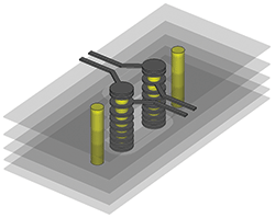
Figure 1 A microstrip-to-stripline transition implemented with vias. The two outer vias are stitching vias, which provide a path for the return current.
This article will show how 3D electromagnetic simulation can be implemented in the design flow for high speed serial channels. It will show how to optimize reference plane changes and make early design decisions such as layer stackup, via back-drilling or trace separation that are difficult to change later. At the other end of the design process is the verification/sign-off stage. One problem that plagues sign-off engineers is that not all components of the transmission channel are under their control and high fidelity simulation models of those components can be hard to come by. What to do in such cases and how to make reasonable assumptions about unknown components will be covered.
Signal integrity (SI) is of critical importance in modern electronic devices. Increasing speeds and the widespread adoption of mobile devices mean that two trends are increasingly dominating electronic design: an increase in frequency and a decrease in board size. These are changing the design workflow, as engineers need to account for effects that could previously be ignored.
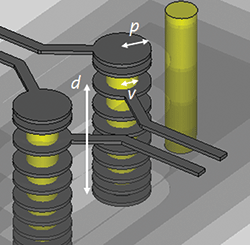
Figure 2 The three design parameters: pad radius (p), via radius (v) and via stub length (d).
Insertion loss is typically greater at higher frequencies and, to counteract this effect, emphasis and equalization are used. At the transmitter, the signal can either be filtered (de-emphasis) or amplified (pre-emphasis) in such a way that the insertion loss is counteracted. Both have their drawbacks: de-emphasis can cause noise problems by reducing the signal amplitude, and pre-emphasis can lead to emissions issues. For this reason, modern technology increasingly uses equalization where the signal is filtered immediately before the receiver.
Emphasis and equalization are difficult to implement for parallel channels, since each receiver requires a separate equalizer module, resulting in larger/more expensive ICs and higher power consumption. In addition, parallel channels limit the minimum size of the electronics, and bringing many traces together increases the crosstalk problems. These are some of the reasons modern high speed transmission channels such as PCI, SATA, USB and HDMI are often implemented as serial channels using serializer/deserializer (SerDes) technology.
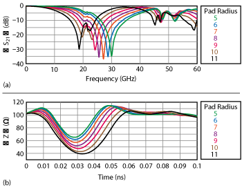
Figure 3 Insertion loss (a) and TDR response (b) vs. pad radius.
Unlike single-ended parallel transmission lines, serial channels are usually differential. This article explains how a serial channel can be designed and characterized using simulation to verify that it meets signal integrity specifications, starting from the design of the vias through the full simulation of the board, including sockets, packages and cross-talk.
VIA DESIGN
Being routed on an inner layer of the PCB helps shield the trace. However, components are mounted on the surface of the PCB, so vias are used as transitions between the surface microstrip and the deeper stripline layers (see Figure 1). The via represents a transition between two transmission lines and must be carefully designed to minimize reflection. A balance must be struck between signal integrity and manufacturing cost.
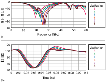
Figure 4 Insertion loss (a) and TDR response (b) vs. via radius.
To investigate how the design parameters affect the performance of the vias, a study was carried out using a time domain EM solver in CST STUDIO SUITE®. The parameters investigated were pad radius, via radius and back-drilling (see Figure 2). In each case, a parameter sweep was performed to calculate how these parameters affect the insertion loss and TDR response (see Guide to Terminology sidebar). The via initially shows a resonance in the insertion loss at around 24 GHz, which could lead to signal integrity problems. Increasing the size of the via pad increases the capacitance of the via (see Figure 3); changing the size of the pad shifts but does not remove this resonance. Changing the via radius has similar effects (see Figure 4), as the via radius controls its inductance.
 To deal with this resonance more effectively, back drilling is considered. Back drilling removes the unnecessary via stub, which is the source of the resonance. A simulation shows that back drilling to remove the stub entirely almost flattens the TDR response (see Figure 5). The drawback of back drilling is increased manufacturing cost. As an alternative, the stripline could be routed on a much lower layer of the PCB. This would decrease the effective length of the via stub and reduce the resonance without the additional drilling. The benefit of this from a signal integrity perspective can be seen by looking at a simple channel. If it is assumed that the trace is a stripline with vias at each end, it can be simulated as a system to calculate its eye diagram, using I/O buffer information specification (IBIS) models. Data standards specify allowable eye opening values for channels to ensure SI performance, and the components need to remain above those values. Optimizing the via has increased both the eye height and width and offers more leeway to add additional components to the channel (see Figure 6).
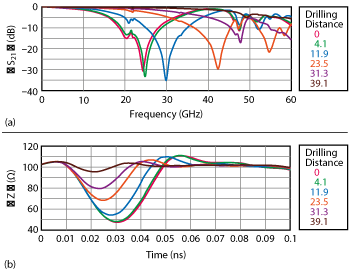
Figure 5 Insertion loss (a) and TDR response (b) vs. drilling distance to vary the stub length.
BUILDING THE CHANNEL
With the traces laid out, the next step is to build the rest of the channel. Where a channel crosses from one board to another, there needs to be a connector or socket. In this case, a PCI Express socket (see Figure 7) is used to connect the riser card to a motherboard. In some cases, a 3D model or an S-parameter model of a component is available from the manufacturer and can be implemented in the design directly. In other cases, the component might need to be modeled within the simulation software or characterized through measurements. In this case, the PCI Express connector is modeled while the motherboard is represented by a length of stripline. These were linked together using the circuit simulation solver in CST STUDIO SUITE®, which allows 3D models and analytical circuit elements to be combined. Adding the socket and the motherboard reduces the eye height to 278.0 mV, which is a significant drop compared to that seen when the stripline was kept to a single board (see Figure 8).
In a real PCB, the exact route of the traces is also important, especially when taking crosstalk into account. The spectrum of high speed signals extends to very high frequencies — the fifth harmonic of an 8 Gbps signal is at 20 GHz. At these frequencies, the return currents in the reference planes have a severe impact on the signal integrity; even individual pads can cause unexpected resonances. Only full wave 3D solvers model these effects rigorously. In this particular case, a channel which includes a riser board (with a stripline trace and the vias), a socket and a motherboard are considered, with several transitions that can affect the signal. Taking the 3D structure of the PCB (see Figure 9) into account reveals that there is a noticeable effect on the eye diagram — the eye width is reduced again to 72.5 ps and the eye height to 252.8 mV. This would not have been detectable using a simplistic analytic trace model.
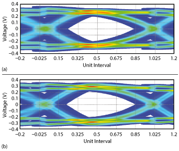
Figure 6 Eye diagrams for a simple 8 Gbps channel with two vias before (a) and after (b) via optimization. The eye opening is 75.62 ps wide and 401.8 mV high before optimization, and 78.75 ps wide and 419.3 mV high after.
In this case, there are additional differential pairs on either side of the channel, driven by the same devices and acting as aggressors. Taking these into account is a matter of adding additional ports to the simulation. 3D simulation is critical here, as the exact separation between the traces across their entire length and especially near discontinuities will have a massive impact on the crosstalk. When the simulation is repeated with the aggressor channels included, it was found that the eye has closed even further (see Figure 10). The width of the eye is now 65 ps, with an eye height of 206.9 mV. Compared to the bare stripline, the introduction of transitions, the consideration of the realistic 3D traces and the inclusion of crosstalk effects has revealed that the actual SI performance of the channel is significantly different.
With the full channel modeled, one more important figure of merit can be calculated. This is the timing bathtub, which shows the expected bit error rate (BER) at different sampling times (see Figure 11). The eye width determines the width of the bathtub. In this case, the channel still meets PCI Gen 3 specifications, but in other cases the channel will need to be rerouted or otherwise modified to improve its transmission characteristics and reduce crosstalk.
CONCLUSION
The performance of a high speed digital SerDes channel is dependent on the performance of every part of it, from the traces and the connectors to the transmitters and receivers. Identifying and mitigating potential SI problems early in the design process can save time and money later on, but these SI problems can depend on complex couplings that can only be identified by full 3D electromagnetic simulation. These include the back drilling of vias, the quality of the connectors, the routing of the traces and the chips that drive the channel. All of these can be considered by simulation, allowing the performance of the entire system to be analyzed.
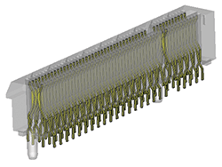
Figure 7 Simulation model of a PCI Express connector.
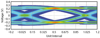
Figure 8 Eye diagram for a channel including a PCI Express socket and two vias. The eye opening is now 73.12 ps wide and 278 mV high.
Figure 9 PCB simulation model showing several PCI Express traces (highlighted).
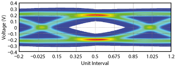
Figure 10 Eye diagram for the full channel including crosstalk. The eye opening is now 65 ps wide and 206.9 mV high.

Figure 11 Bathtub curve for the full channel, including crosstalk.