
Figure 1 "Lobster claw" high frequency connector design.
Historically, coaxial connectors have had two methods for center conductor mating, the hermaphroditic contact and the male pin/slotted female contact. The non-sexed connectors have many advantages, the main being that only one connector type is required. As frequencies got higher, connectors became smaller in order to remain single mode. The success of the SMA connector foretold the end of the non-sexed connectors. Mechanically it is difficult to make butt type connectors. The pin depth tolerances are very critical and the small size makes it difficult to make a resilient contact. These factors raise the cost of the connectors well above the simple male pin/slotted female contact.
As connectors became smaller and reached higher frequencies, the male/female contact design became the standard. A slotless female design was introduced for metrology applications, but this became impractical above the 50 GHz, 2.4 mm connector. A four-slotted contact is much more resilient. The 3.5 mm connector, designed to mate with SMA, incorporates a four-slot female contact and an air interface. This results in a higher precision design, but with a problem. Since they have to be compatible with the SMA connector, the size of the male pin was set at 0.914 mm (0.036"). The center conductor size of the 3.5 mm connector is 1.52 mm (0.060"). Therefore, the wall thickness of the female fingers is 0.3 mm (0.012"); this is quite thick for such a small diameter. After slotting, the fingers are closed and the part is heat treated. If they are closed too little, the contact will be unreliable. If they are closed too far, the insertion force required to mate the connectors will become quite high. This introduces excess wear and may even distort the support beads holding the center conductors in place. The large wall thickness also introduced more pin gap reflection. The impedance of the gap section is 80 ohms.
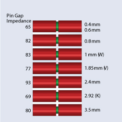
Figure 2 Pin gap impedance values.
The 40 GHz, 2.92 mm K connector, introduced in 1985, addressed many of these problems. A short male pin ensures that the outer conductor parts align the two connectors before the center conductors engage, so the male pin will not damage the female by being inserted at an angle. The center conductor diameter of the K connector is 1.27 mm (0.050") leading to a finger wall thickness of 0.18 mm (0.007"). This means that the fingers are more flexible and the insertion pressure is greatly reduced. As a result, K connectors are rated for 4000 connections.
The 50 GHz, 2.4 mm and the 65 GHz, 1.85 mm connector interfaces were introduced by HP/Agilent (now Keysight). The 2.4 mm connector was required with introduction of their 50 GHz VNA. With improvements of V connector bead design, the VNA frequency moved up to 65, then 67, and now 70 GHz.
The 110 GHz, 1 mm connector was introduced by Agilent (now Keysight). Anritsu introduced the 110 GHz W connector with the introduction of their 110 GHz broadband VNA. Anritsu has also introduced a 0.8 mm connector as part of the 70 kHz to 145 GHz VNA and is working on even higher frequency connectors.
THE SLOT PROBLEM
If the dimensions are reduced by 50 percent for a higher frequency connector, the slotted female contact would be very fragile. If a thin walled design was used, the insertion force would be very slight, but so would the contact pressure. If a thick walled design was used, the contact pressure would be greater but the finger flexibility would be minimal. So a slotted female contact seems out of the question. An out of the box comment supplied the answer. “Don’t slot the female, slot the male pin. What would that look like?”
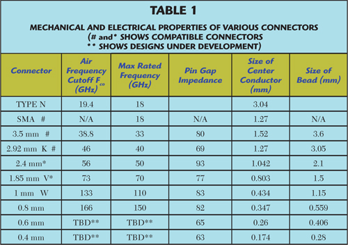
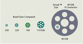
Figure 3 A comparison of sizes of the beads since the K connector.
We can make the female wall very thin so there are no slots. Therefore the male pin could be large, closer to the main center conductor size, as shown in Figure 1. This pin could be made with a 0.05 mm slot. Also since the slotted portion is contained inside the un-slotted hole, it would be quite robust with no tendency to spread out like the standard slotted female contact. The impedance of the pin gap is 65 ohms, much less than lower frequency designs. This makes the connector less sensitive to pin depth reflections (see Figure 2). Table 1 provides information on existing connectors and those in design. The current plan is to use the new slotted male design (called the “lobster claw”) in the sub-0.8 mm connector designs. Notice that the center conductor of these connectors quickly approach 1/20th the size of the N connector center conductor.
CONNECTOR SIZES AND IDENTIFICATION
Traditionally, connectors moving up in frequency get smaller. Anritsu decided to keep the coupling nuts of new connectors the same size as the 1 mm connector. Smaller than that makes the connectors difficult to work with. Also, the threads are different. The 1 mm connector has a course thread and the higher frequency connectors have a fine thread. It is critical that all of the sub-1 mm connectors cannot be connected in a destructive manner.
The connectors are identified by a laser engraved number that shows the connector size. The number is also etched on the coupling nuts. The
1 mm male coupling nut is plain, the 0.8 mm coupling nut has a single groove and smaller connectors have sequentially additional grooves.
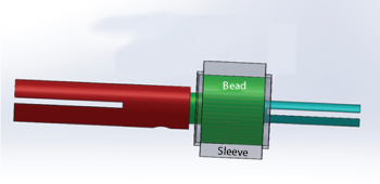
Figure 4 Swaged bead sleeve drawing.
SUPPORT BEADS
The connectors above the 1 mm connector have a maximum rated frequency that is the same as the Fco, the air dielectric cutoff frequency. The lower frequency connectors have support beads that are larger than the air outer conductor size. This means that they have an Fco that is substantially lower than the air Fco. The cutoff frequency is inversely proportional to the square root of the dielectric constant of the material between the center conductor and the outer conductor. The new designs have support beads that are substantially smaller than the size of the air outer conductor. They are designed to have an Fco that is the same frequency as the air Fco. They are also much smaller, as shown in Figure 3.
A major problem with making the bead size smaller than the air dielectric outer conductor size is how to captivate the bead. The old designs, where the bead is larger than the air outer conductor, allowed a mechanical capture in both directions. The solution was a sleeve that contained the bead and had an outer diameter about the same size as the air outer conductor. The sleeves have very thin lips on both ends and are swaged to hold the bead in place (see Figure 4). The assembly can then be soldered in place, due to the use of high temperature plastics.
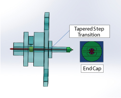
Figure 5 0.8 mm connector design.
ASSEMBLY DETAILS
Figure 5 shows a 0.8 mm connector and does not have the lobster claw design. The backside of the connector is a Coplanar Waveguide (CPW) design similar to a wafer probe. The center conductor is common, but the outer conductor end cap can be configured to accommodate different CPW designs. Figure 5 also shows how the bead sleeve is soldered into the outer conductor.
A feature of the design is the ability to adjust the position of the back side CPW interface. Correct positioning of the connector to the substrate is critical to performance. Holes are centered at the edges of the flange. A tapered pin allows the flange to be moved up and down as well as left and right. When the connector is properly connected to the CPW substrate, the flange screws are tightened.
These types of connections are mostly used to connect high frequency VNA modules to a wafer probe that in turn will be used to measure CPW substrates over a very large bandwidth. VNA technology is now available from 70 kHz to 145 GHz using 0.8 mm connectors. Waveguide modules extend that coverage to 1.1 THz. These “lobster-claw” connectors are intended to extend the broadband coverage from 70 KHz to 332 GHz.
CONCLUSION
What will be the last connector in a long string of higher and higher frequency connectors?
In 1983, a 40 GHz coax connector was considered unlikely. Today we are designing a connector that reaches almost 10 times higher in frequency. Circuit designers seem to be able to create devices that operate at ever-higher frequencies, and some kind of connection is always needed to make these devices useful. Let’s not limit our imagination.