

The third Electronic Design Innovation Conference (EDICON), was held Oct 17-18, 2018 in Santa Clara. The attendees were treated to two days of technical talks, tutorials and tradeshow with the overlapping topics of RF, SI, PI and EMI. This is a unique combination, allowing cross fertilization between these otherwise separate fields.
Like all conferences, this one offered a chance for colleagues in the industry to catch up with the state of the art, and each other’s careers. Figure 1 shows one gathering of industry experts.

Figure 1. A gathering of industry icons. From left to right: Hilary Lustig, Teledyne LeCroy, Eric Bogatin, Teledyne LeCroy, Bert Simonovich, Lamsim Enterprises, Steve Sandler, Picotest, Ransom Stephens, Ransoms Notes and Janine Love, Czar of EDI CON.
In addition to catching up with who’s doing what and taking a reading of the pulse of the industry, I attend these sorts of conferences because I always learn something new. This year was no exception. The following are some of the things I learned at EDICON 2018:
One of the common (pun intended) themes in the power integrity sessions was how to push the 2-port low impedance VNA technique to the ultra-low impedance range. Brian Hostetler, Cray, Inc., in his talk, 100 uOhm Probing Methods, put in perspective why this is an important measurement.
Just one VRM in Cray’s super computer daughter board supplies more than 200 A at 1 V to the rail on just one device. The load impedance is 5 mOhms. Their specification is a target impedance 5% of this, or 250 uOhms. This means they need to measure the components of the PDN impedance to a small fraction of 250 uOhms.
The challenge identified by Steve Sandler and Anto Davis, both with Picotest, is the ground loops from the cables when they are connected together at the VNA. This is illustrated in Figure 2.
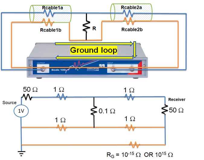
Figure 2. The ground loop connections and its equivalent circuit which includes the impedance of the cable shields, dominated by their resistance.
A typical 2-port measurement will include the series resistance of the cable return path. When the DUT impedance is very small, and there is a low resistance in the common return path back to the port 1 ground reference, additional currents can flow in the large parallel ground loop, unrelated to the DUT. This common path must be blocked by some sort of common mode choke in order to get an accurate low impedance measurement.
When a common mode choke is added to the measurement at port 2 to prevent the ground loop currents, Sandler reported being able to measure impedances as low as 20 uOhms, as shown in Figure 3.

Figure 3. Measured impedance of a low resistance reference showing 20 uOhm.
I had the honor and the privilege of working with Steve Sandler and Larry Smith on two papers related to PDN design. In our first paper, PDN and Target Impedance, we reviewed three limitations of using just a simple target impedance as the spec for designing a PDN.
The first problem is it does not include the noise from the VRM. This will eat into the noise margin. Secondly, any peaks in the PDN will contribute ringing from step current responses. Generally, the impedance of the peaks must be close to the target impedance. Finally, if there are multiple peaks in the PDN, even if they are each below the target impedance, a rogue wave of periodic current loading with just the right sequence of frequencies, phase and duration, could generate more PDN voltage noise than allowed in the spec. An example of a rogue wave measured in a PDN is shown in Figure 4.
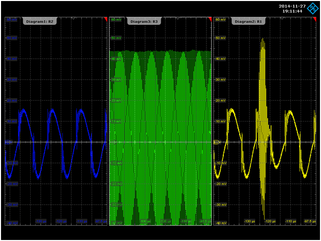
Figure 4. An example of a rogue wave created from two sequential excitations of PDN peaks. The peak voltage noise is larger than from either wave alone.
In our second paper, VRM Modeling: A Strategy to Survive the Collision of Three Worlds, we reviewed the three popular models for a VRM. A VRM model is important to simulate the impedance profile of the entire PDN. The LRLR model is the best compromise, as a simple passive model of a VRM which accounts for the DC output resistance and the damping term with the bulk capacitor.
But, this model does not include any information about how the VRM noise contributes to the self-aggression noise resulting from transient currents on the die. A state-space, active model is needed which includes both the passive impedance of the VRM and the switching noise it might create. Figure 5 compares the three models with a measured example. If just the PDN impedance profile is important, the RLRL model is a good compromise.

Figure 5. Comparison of the three impedance models of the PDN and a measured example. The simple RL model will miss either the parallel resonance damping or the DC output resistance of the VRM.
Al Horn and colleagues at Rogers Corp, introduced a new material system, MAGTREX™ 555 laminate with high permeability as well as high permittivity. This polymer composite material has an effective ur = 6 and Dk = 6 and an effective index of refraction of 6. In addition to having a higher index of refraction enabling smaller antennas, it also has the unique advantage of an impedance, based on the sqrt(ur/Dk), that matches free space. This makes it a more efficient radiator.
With its higher index of reflection in the 100 MHz region, it can enable significant miniaturization of patch antennas and filters whose dimensions scale inversely with the index. An example of a smaller sized bandpass filter made from this new laminate, is shown in Figure 6.

Figure 6. A small size filter using the new high permeability, low loss laminate.
HeeSoo Lee of Keysight offered another metric to use when analyzing the properties of vias. While we usually plot the return loss of a via, Lee proposed using the transformed input impedance in the frequency domain. In his paper, Via Characterization and Modeling By Z-Input Impedance, he showed that the input impedance gives immediate insight into whether the via is inductive or capacitive.
Lee said the input impedance in the frequency domain is just another metric, like TDR in the time domain, for a via embedded in a 50 Ohm environment. Figure 7 compares the two different ways of displaying the input impedance.
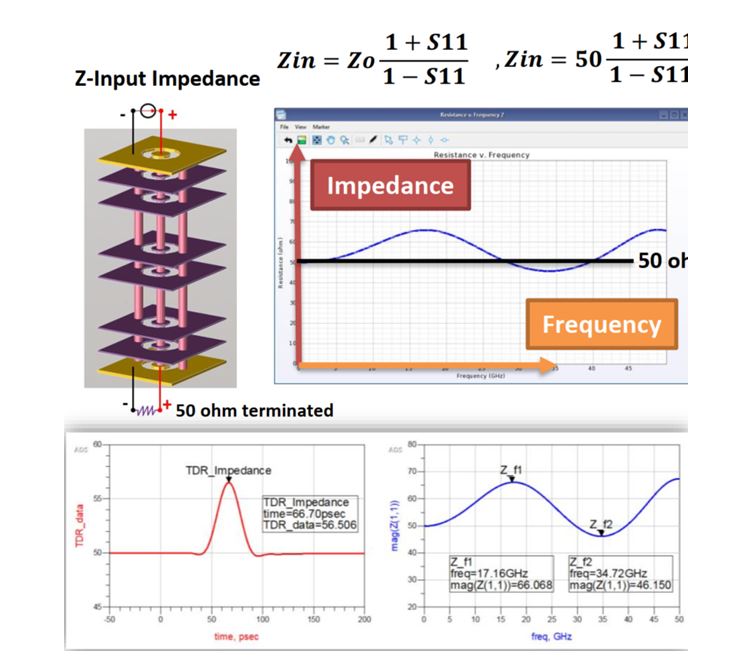
Figure 7. The two ways of displaying the input impedance of a via, in the time domain and the frequency domain.
When optimizing the features of a via to be more transparent, using the input impedance in the frequency domain as the target can offer a faster path to optimized via design.
Tom Clupper and colleagues from W.L. Gore, in their talk, Cut-off frequency Prediction for MMW Coaxial Interconnects, explained a key ingredient to accurately simulate the various modes of a coaxial transmission line.
We usually use the TEM00 mode of a coax for signal propagation. This has the lowest loss. At low frequency, this is the only mode that will propagate. But, as frequency goes up, the TE11 mode will be the first one excited. The key message from their talk is if you want to simulate the onset of these higher order modes, you must introduce some asymmetry in the simulated geometry, which will cause signal from the symmetrical TEM00 mode to couple into the asymmetrical TE11 mode. Figure 8 shows these modal geometries.
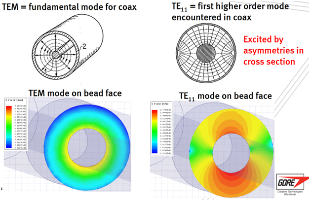
Figure 8. The TEM00 and TE11 models of a coax. Note an asymmetry is needed to simulate modal conversion.
In all real cables and connectors, small manufacturing defects provide the asymmetries to stimulate mode conversion. This mode conversion is the reason 3.5 mm connectors are limited to 26 GHz when filled with air or 18 GHz when filled with PTFE.
Jay Diepenbrock and colleagues on the IEEE P370 specification working group presented two summary talks on the progress of the P370 specification and a preview of some of the tools which will soon be released. This specification is related to describing how a DUT is de-embedded from a measurement of the fixture-DUT-fixture structure. The specification will include a metric to evaluate the quality of the 2x thru fixture, a metric to compare two S-parameter files, like a measurement and a simulation or an original DUT and a de-embedded DUT, and a metric to evaluate the quality of an S-parameter model. This quality metric will measure the passivity, reciprocity and causality of an S-parameter file.
Bert Simonovich, in his paper, Practical Channel Modeling for High-speed Design, showed how he can take just the information available in the engineering datasheets of the laminate materials and copper foil Rz roughness, with the as designed geometry of a channel and accurately predict performance. No fitting and no test coupons are necessary.
Combining the dielectric materials and the copper foil roughness as measured on a surface profilometer, his model calculates the effective Dk of the core and pre-preg, and the losses from the dielectric and copper. Using an FCI ExaMax backplane as an example, he compared the measured insertion loss of a channel with his open loop simulated insertion loss using datasheet information as input. Figure 9 shows the excellent agreement he is able to obtain.
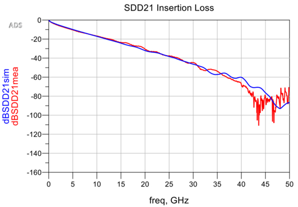
Figure 9. Comparison of the measured and simulated insertion loss of a long backplane interconnect using just datasheet information.
I stopped by the Ansys booth and learned from Mark Ravenstahl, Technical Director of Strategic Partnerships, about a new feature in the latest HFSS release, v19.2 which incorporates a hybrid solver. This feature is called “HFSS Regions in SIwave.” Normally, SI wave is a boundary element 2.5 D solver. Its strength is transmission lines across the board that might encounter some trace width changes or return path discontinuities.
It does not handle 3D structures very well, like via fields, bond wires and packages. By identifying these structures as HFSS structures, critical net simulations can be completed directly in SIwave which calls HFSS to complete the more complex 3D structures.
For example, in a net, as shown in Figure 10, with packages and via fields at either end of the uniform transmission lines, the solver will automatically select HFSS to simulate the S-parameters of the 3D regions and use SIwave for the uniform regions. This provides the optimum balance between accuracy and computation time.
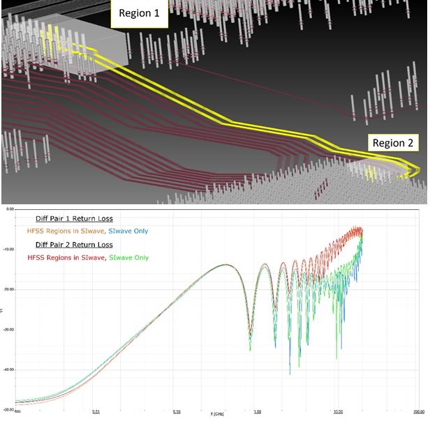
Figure 10. Top: a complex trace with connection to via fields. Bottom: comparing the simulation results with just SI wave and with the new hybrid solver. HFSS predicts the higher return loss above 3 GHz from the via field.
Steve Krosswyk, New Product Signal Integrity Engineer with Samtec, walked me through a backplane, shown in Figure 11, running at 2.2 Tbps, using 80 lanes at 28 Gbps NRZ per lane. This backplane had been running nonstop for about 4 hours since it was turned on in the morning. More than 5,000 Terabytes of data had been transmitted error free in the loop back.

Figure 11. Top: 2.2 Tbps backplane running at 28 Gbps NRZ per lane. Note the use of fly over cables for some of the long, intra-board interconnects in the bottom figure.
It is rare to have one conference with elements of RF, SI, PI and EMC applications under one roof. As these fields blur together in many applications, the cross fertilization between these normally separate worlds will be a useful feature of the EDICON conferences.
Selected papers from the conference will be reprinted in the SI Journal over the next few months.