
There are topics where even well-seasoned signal-integrity experts cannot agree on a unified answer. Probably one of the few exceptions is via stubs. We all tend to agree that high-speed signals are significantly degraded if the resonance frequency of a via stub attached to the signal path comes close to the signaling frequency. In contrast, we are usually not worried about having via stubs on power and ground planes and shapes. Does it mean they are completely harmless? The interesting answer is that when it comes to potential damage to high-speed signals, power-via stubs can be almost equally as bad as signal-via stubs. Here is how and why.
First, let us look at the basics. In the RF-microwave nomenclature, a stub is a transmission line that leads ‘nowhere.’ In other words, it is a dead end for the intentional signals we want to send around our system. In RF and microwave engineering, stubs have a very important and useful role in creating filters and shaping the frequency response of circuits. In signal integrity, stubs are usually considered as an unintentional side effect of the physical implementation. They can create signal degradation [1], though in rare cases they can be useful in signal integrity, too, such as when we create intentional capacitive loading or capacitive compensation with short mismatched or unterminated traces [2].
A piece of uniform and loss-less transmission line can be characterized by its inherent capacitance and inductance, C and L, where for the loss-less case we can assume that C and L are frequency independent scalar values. From C and L we can define two basic parameters: a Z0 characteristic impedance as the square root of L/C and a tpd propagation delay as the square root of L*C.
With these definitions, the propagation delay is the time of flight of the electromagnetic wave through the interconnect and the characteristic impedance is a value such that if we terminate one end of the interconnect with this resistance, the input impedance looking into the interconnect at the other end will show the same resistance value, regardless of the test frequency and regardless of the length and delay of the interconnect. We can also remember that this observation steers us to use scattering parameters at high frequencies. The situation of course becomes more complicated if losses cannot be ignored: C and L become complex-valued frequency dependent parameters. However, to understand the impact of stub resonance, modeling them with a loss-less transmission lines will properly capture the essence of the potential problem.
Figure 1 shows how the input impedance of the loss-less transmission line varies if the termination resistance does not match the characteristic impedance. For this example, we assume a 60-ohm loss-less trace. The input impedance is frequency independent 60 Ohms only when the termination resistance is 60 Ohms. For any termination resistance value at very low frequencies, the input resistance equals the termination resistance. This is what we expect from common-sense assumptions, because the loss-less transmission line behaves like a short between the input and output signal terminals. As the frequency goes up, we notice that impedance lines starting above 60 ohms begin to drop, whereas response lines starting at lower values begin to curve upwards. Eventually all response lines reach an inflection point and an extremum, maximum or minimum, beyond which the trend reverses and becomes periodic.

Figure 1: Input impedance test setup on the left, magnitude of a loss-less uniform 60-ohm 10”-long transmission line with different values of resistive terminations on the right. Note the logarithmic horizontal scale.
The first extremum frequency in our case is around 150 MHz. This is the frequency where four times the propagation delay equals the period of excitation. This is the quarter-wave resonator case, and a circuit operating at this frequency can also be called inverter, because it ‘inverts’ the termination resistance (or impedance in the general case): at the quarter-wave resonance the input resistance becomes the characteristic impedance squared divided by the termination resistance:

For a generic ZT termination impedance, the input impedance of a loss-less transmission line can be expressed as

where l is the length of the interconnect and b is the propagation constant. For the loss-less case b is the radian frequency multiplied by the propagation delay. Viewed differently, the bl argument of the tangent function is the phase shift of the signal between the input and output terminals.
From the input-impedance formula we can tell that dependent on the values of ZT termination and bl argument, the expression can produce zero or infinite values regardless of the characteristic impedance. In fact when we leave the end of the stub open and ZT is infinite, we get zero input impedance at an infinite number of frequencies, first when bl becomes 90 degrees.
This is the quarter-wave inverter at its extreme, when the open termination at selected, frequencies gets transformed to zero input impedance. This phenomenon can happen at any actual physical length; what matters is that the bl electrical length has to satisfy the quarter-wave resonance. It can happen in mile-long power transmission lines and in tiny microvias alike, the difference is just the frequency where it happens. Losses in the transmission line forming the stub will result in a finite minimum resistance instead of a dead short, but as long as the characteristic impedance of the stub and the transmission line it gets attached to have the same order of magnitude, even a lossy via stub can produce low enough impedance at the quarter-wave resonance that the signal gets severely distorted.
In signal integrity, through-hole metallization of multi-layer boards that connect only two internal layers create open-terminated stubs by the unused portion(s) of the via barrel. At the quarter-wave resonance conditions (and at their appropriate harmonics and in a certain frequency range around them) the low input impedance of the via stub shunts the signal path, distorting the frequency response and creates a notch (see Figure 2).
Unless the stub is exactly at the receive point, even a complete shunting of the signal path does not necessarily mean that the received signal is entirely killed, but most of the time it gets severely distorted.
Now that we understand how via stubs can degrade high-speed signals, we can look at via holes on power and ground nets. The biggest difference between signal nets and power/ground nets on our typical large PCBs is that we use traces (with characteristic impedance in the tens of ohms) for signaling, and we tend to use planes or plane shapes (with an approximately two orders of magnitude lower equivalent characteristic impedance) for distributing power. The vertical via connections, on the other hand, do not have this wide spread of dimensions. The length of signal and power vias alike is dictated by the board thickness, and their diameter does not follow the orders of magnitude difference in net impedance. We may use somewhat bigger drills for power and ground connections, but not ten or hundred times bigger bigger drills.
Based on these observations, we can conclude why stubs on power/ground vias do not create problems on the power/ground nets. Simply the vias are too ‘small’ and ‘weak’ to make any noticeable impact on the physically much bigger and low impedance power/ground nets.
But power via stubs may still matter for SI. When structures resonate, the oscillating fields around them can create a large area of influence [3], [4]. Structures (traces, vias, pins) which are properly spaced for a given crosstalk coupling value, can experience almost full coupling under resonance conditions. But the most important realization is that the resonance does not care what our intention with the structure was. So it is true that the resonating via stub can hardly influence a power net, but the resonance is still just a resonance. It creates large fields that can couple to nearby structures, including signal nets.
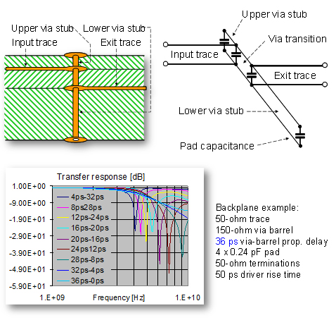
Figure 2: Via stub illustration. Top left: PCB construction, top right: a simple electrical model with transmission lines, bottom middle: transfer response as a function of exit-trace height in the stackup. In the legends, the first number is the via-transition delay, the second number is the stub delay.
As an example, we look at a via pair with a non-driven via in between. (Note that I do not call the non-driven via a return via, because all what matters in this case is that we do not drive this via with intentional signals.)
We assume that the non-driven via is attached to a power plane close to the top of the stackup, as shown in Figure 3. For sake of simplicity the assumed board stackup has only four layers. The vias have 10 mil diameter, 15-mil pads and 20-mil antipads and 113 mil vertical length. The dielectric is assumed to be low-loss, as shown by the material definitions ‘core’ and ‘prepreg’ in Figure 4.
The vertical dimension details are shown in Figure 5. Note that in this simple illustration the middle of the stackup is ‘empty’, there are no other layers there. In a realistic multi-layer printed circuit board of this thickness we would see multiple layers occupying the center of the board stackup. However, if there is no electrical connection from the other layers to any of these vias, those layers will have only a slight capacitive loading effect, increasing the propagation delay and lowering the average via impedance, but will not alter the resonance effect much more. Note also that this simulation problem is not well localized because there is no direct connection inside the structure between the plane layers in the top and bottom; the connection is left to the boundary conditions used by the simulator.

Figure 3.: 3D geometry view of a signal via pair with a non-driven through-hole.

Figure 4: Material definitions.

Figure 5: Vertical stackup dimensions.
We simulate this very simple structure in a 3D solver, with ports 1 and 3 attached to the left via top and bottom connections and ports 2 and 4 attached to the right side via top and bottom connections. The short horizontal lead-in traces are approximately 50 ohms in impedance. The input reflection (S11) at Port 1, the main signal transfer (S31), near-end crosstalk (S21) and far-end crosstalk (S41) are plotted in Figure 6.
Up to about 10 GHz, things look reasonably good: the loss in the main path is fairly minimal (the actual value is -0.25 dB at 10 GHz), though the reflection gets above -20 dB beyond 4.5 GHz, which is due to the simple fact that these vias have not been optimized for reflection. The crosstalk terms are approximately 20 dB below the reflection.
However, at and near 13 GHz, the behavior becomes very bad: there is a sharp dip in the transfer function (S31, red trace) and there is a very big peak in both crosstalk terms (S21, green trace and S41, black trace). The frequency of the notch and crosstalk peak, 13 GHz, corresponds to the quarter-wave resonance of the non-driven via stub. The vertical length of the stub is 106.5 mils, and since most of this length goes through the core material, we can use Dk = 3.8 for the dielectric constant surrounding the via. The corresponding unloaded propagation delay is 17.6 ps, which gives us a first-cut estimate for the quarter-wave resonance of the via stub as 1/(4*tpd) = 24.2 GHz. The difference between the calculated 24.2 GHz and simulated 13GHz is due to the electrical loading of pads and plane antipads.

Figure 6: S parameters of a via pair with a nearby power via stub.
The corresponding time-domain response is shown in Figure 7. The input TDR and through TDT responses are clipped on the vertical axis to allow us to see the crosstalk waveforms with better vertical resolution. There is a ringing on the quiet via with very low damping. Note that the near-end and far-end waveforms are very close to opposite phase.

Figure 7: Time-domain response of the structure shown in Figures 3 through 6.
The solution to this potential problem is the same as for via stubs in the signal path: when they create problems, we need to eliminate them or need to push their resonance frequencies out of the sensitive frequency range either by backdrilling or by using blind or buried vias, or simply by moving them further away from sensitive signals.
Finally, we can conclude that ground vias are less likely to create this kind of problem because in multilayer boards we tend to have multiple ground layers, which break up the via stubs to shorter sections and this will push their resonance frequencies higher.
References
[1] Bert Simonovich, “Via stubs Demystified,” available at https://blog.lamsimenterprises.com/2017/03/08/via-stubs-demystified/
[2] “Loaded Parallel Stub Common Mode Filter,” DesignCon 2008, Santa Clara, CA
[3] “Examining the Impact of Power Structures on EM Model Accuracy,” DesignCon2011, Santa Clara, CA, January 31 - February 3, 2011
http://www.electrical-integrity.com/Paper_download_files/DC11_8-TA3_Miller-paper.pdf
[4] “Crosstalk In Via Pin-Fields, Including the Impact of Power Distribution Structures,” DesignCon2009, Santa Clara, CA, February 2-5, 2009,
http://www.electrical-integrity.com/Paper_download_files/DC09_7-WA1--Gustavo_Blando.pdf