Challenges to Consider for High-Speed-Digital (HSD) PCB Design and Layout
Nearly all circuit design aims at progress in one direction: smaller printed circuit boards (PCBs) with more functions, higher speeds, and higher frequencies. The high circuit densities associated with such enhanced PCBs pose many design and fabrication challenges for high-speed-digital (HSD) circuits. As circuits shrink and bit rates increase, achieving acceptable signal integrity (SI) requires experience and creativity. It calls for foresight in layout planning to keep signal paths short, which helps minimize interference between closely spaced circuits. Circuit materials must support electrical and mechanical design specifications, and components must be selected for optimum size and placement. All these factors combine to create many challenges when developing an HSD PCB.
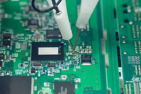
Fortunately, with modern computer-aided design (CAD) tools, the performance of any PCB layout can be simulated before it is physically implemented as a prototype. Once the prototype is attempted, effective use of inspection equipment and manual test and automated test equipment (ATE) systems can be added to an optimized PCBA that meets the latest requirements for reduced size, weight, and power (SWaP). Learn how the methods practiced by an experienced design and fabrication team can provide high yields even with the most challenging HSD circuit layout requirements.
Impedance Control and Differential Signaling in High-Speed Design PCBs
Layout is critical to the quality and performance of HSD PCBs, which are categorized as circuits transferring signals above 50 MHz. Many variables can affect SI in multilayer PCBs with HSD circuits, including component placement, positioning of power and ground planes, and the number of transitions between circuit layers. Layer transitions add a certain amount of mismatch loss to the total interconnect path length, and it is advantageous to keep the number of transitions to a minimum. Even the signal lines are inherently lossy; the loss only increases with increasing frequencies and data rates. The lengths of these signal paths should be minimized where possible, and when longer signal paths are required, they should be fabricated on an appropriate low-loss circuit material.
Impedance control is crucial in creating HSD PCBs with low transmission-line losses. High-frequency transmission lines, for example, are typically matched to a characteristic impedance of 50 Ω to minimize signal reflections, losses, and distortion. The same practice supports AC flow with minimum loss even at high data rates. It requires precisely matched signal trace widths and conductor materials, and even variations in the dielectric circuit material's thickness can result in variations in the nominal transmission-line impedance.
Differential signal pairs rather than single-ended signal lines are often used to minimize phase noise, signal distortion, and electromagnetic interference (EMI) in HSD PCBs. Differential signal pairs effectively support high-speed protocols such as PCIe or Ethernet signals.
The general principle behind differential signaling is that the lines of a differential pair experience approximately the same localized signal disturbance, so differential lines are not sensitive to the quality of the ground connections on the PCB. They can transfer much higher data rates than single-ended lines without distortion and bit errors. Serial differential signaling provides effective high-speed communications in HSD circuits for extended signal paths.
Material Considerations for High-Speed Digital Printed Circuit Boards (PCBs)
Selecting circuit materials is an essential early step in creating the foundation for a practical HSD PCB layout. Key parameters to consider when choosing circuit materials for HSD PCBs include dielectric constant (Dk), dissipation factor (Df), coefficient of thermal expansion (CTE), conductor type and thickness, and conductor surface roughness. Circuit materials with low Dk values generally support higher data rates and have faster signal propagation speeds. Circuit materials with the lowest possible Df will suffer minimal signal loss and minimal conversion of signal energy into heat. That heat can damage and shorten the lifetime of a PCB. Because a material's Dk directly correlates with transmission line impedance, materials with Dk consistency help keep variations in impedance and propagation speeds to a minimum. Variations in propagation speeds through a circuit material can result in digital timing skews and possible signaling errors. In general, Dk and Df values should vary as little as possible across operating temperature range and bandwidth for optimum consistency in performance when used within challenging operating environments.
For fast analog and digital signals, current flows close to the conductor's surface, with the depth into the conductor decreasing with increasing signal frequencies or data rates. A conductor's physical width affects its resistance and loss characteristics, with any reduction in its cross-sectional area yielding an increase in its effective resistance. The surface roughness of the copper conductor also affects HSD PCB performance since the current flows close to the conductor's surface. Rougher conductor surfaces result in higher conductor losses.
Another material parameter of concern for HSD PCBs is CTE, which measures how much a circuit material expands with increasing temperature, as might be the case in high-power circuits handling high power levels.
Typically measured in parts per million per degree Centigrade (ppm/°C), CTE values can vary widely for high-frequency/high-speed circuit materials. PCBs fabricated with multiple circuit materials expected to face wide operating temperature ranges require close matching of material CTE values to avoid excessive stress caused by different expansion and contraction rates of the materials. Not to be forgotten, selecting HSD circuit materials requires performing cost-to-performance evaluations on those materials for competitive pricing of the final electronic product.
Guidelines for Component Placement in HSD PCB Design
Once material foundations have been selected, mechanical requirements and electrical performance goals will guide component placement and signal routing for an HSD PCB. While analog components should be placed as close together as possible, the spacing between respective analog and digital components should be adequate to avoid SI problems and harmonic distortion, with typically wider signal traces for analog components than for digital components. Circuit layouts should maintain continuous ground planes as much as possible, especially under sensitive signal traces. More significant components have traditionally been distributed evenly across a PCB to balance the board's weight. Heat-generating components, such as power amplifiers, should be positioned for maximum heat flow through the circuit material and away from the element.
As more functions are added to each layer of a PCB, functional partitioning of a circuit design can provide a practical starting point for placing various analog and digital functions. Isolating components where necessary is effective for EMC control. Grouping components as part of the same functional block can minimize transmission line lengths between components and reduce the required through-holes between circuit layers. Components in packages with large pin counts, such as data converters and microprocessors, need many power traces on a PCB. Placement of complex component packages should always consider the impact of these numerous power traces on surrounding components. Placement of critical components on PCB edges subject to abrasion should be avoided to prevent degrading the performance of those components. Positioning of interface components, such as coaxial connectors, should also consider the ease of access for those who must service the PCB when it is installed in the final product.
 The PCB board checking process by high speed automatic robot system. The high technology electronic component manufacturing process by robotic system. | Shutterstock
Guidelines for Signal Routing in High-Speed Digital Printed Circuit Boards (PCBs)
Once an idea of the component placement for an HSD PCB has been formed, their positions on the board will suggest the first version of the signal trace routing required for connecting those components. The positioning of signal traces should be carefully considered since layouts with HSD signal traces in parallel can suffer the effects of crosstalk, resulting in unwanted signal modulation, distortion, and excessive bit errors. For higher-frequency signals, such as RF through mmWave frequencies, closely spaced signal traces can suffer the effects of passive intermodulation (PIM) when high-frequency signals mix. When placing such lines, it is essential to consider the signal frequencies and power levels. Of course, fine-tuning, such as reducing board size or enhancing SI, will inevitably require repositioning some components or even shifting to a different circuit material, conductor type, or thickness.
Signal routing for HSD PCBs should follow essential guidelines for higher-speed, higher-frequency circuits, such as keeping traces as short as possible, providing transparent access to the ground and reference planes, and avoiding crossing analog and digital signal paths. Sensitive signal lines, such as differential pairs and clock lines, should be allowed additional spacing from other signal lines to minimize distortion. For optimum SI, signal traces should include clear signal return paths on the reference planes. The combination of component placement and signal routing for an HSD PCB layout should also consider the production capabilities of any PCB manufacturer of interest. PCB manufacturers abide by design for manufacturing (DFM) and test design (DFT) guidelines to achieve consistency in their board production processes. By being aware of a PCB manufacturer's requirements, a PCB designer can help speed and simplify the process of building a practical HSD PCB.
Factors to Consider When Choosing a PCB Manufacturer and the Importance of CAD Software Tools
Choosing a PCB manufacturer typically depends upon the facility's capabilities in producing high-frequency, high-speed circuits within a desired set of manufacturing tolerances. For any PCB manufacturing process, variations will occur from lot to lot and board to board, and such tolerances must be acceptable when establishing performance limits for a final electronic product. Some variations will occur because of tolerances in the circuit material, such as variations in the Dk across the board and Dk variations from lot to lot of mass-produced circuit materials. Copper conductors for mass-produced laminates will also suffer variations in thickness, insertion loss, and return loss, and such variations must be part of the HSD PCB planning.
Additional variations occur due to manufacturing processes, such as the location of via holes and through holes and how their locations affect the consistency of the added plating. Some variations in plating thickness are expected from any manufacturing process, which will translate into impedance variations for those signal paths and variations in signal phase and amplitude. The effects of components, circuit material choices, and variations in PCB layouts emphasize the importance and value of CAD software tools before developing a circuit layout or prototype. Commercial CAD tools predict the effects of an almost unlimited number of layout variations, such as the lengths and widths of transmission lines, via hole sizes, plating thicknesses, and board thicknesses. The effects of many structural changes can be analyzed for high-frequency and HSD signals to predict problems for different layouts at different data rates and signal frequencies before committing to any number of circuit materials or components. CAD tools may not eliminate the need for a physical prototype, but they can minimize the number of prototype versions required before production.