
Modeling and measurement of digital serial interconnects is usually done in the frequency domain. That means that the minimal and maximal frequencies (or bandwidth) should be defined even before the analysis or measurement begins. The data rate and rise time define the signal bandwidth and the usual practice is to define the maximal frequency as either the inverse of the rise/fall time (or fraction of it) or as a multiple of the fundamental or Nyquist frequency [1].
Such a simple bandwidth definition may work for some structures, but it may fail for others. Ultimately, an SI engineer must make the decision for a particular signal type and interconnect structure [1]. This paper introduces a simple and practical way to identify the bandwidth with a numerical analysis of defects in a single bit (SBR) or single symbol response (SSR). It begins with a brief introduction into structure and spectrum for 6 Gbps and 112 Gbps signals. Then, it proceeds with analysis of defects in SBR and SSR introduced by the bandwidth deficiency for two practical cases. The bandwidth is defined by a model with an acceptable level of defects in either SBR or SSR.
High-Speed Serial Data Signals
A digital signal in a serial link is a sequence of bits transmitted through the PCB or packaging interconnects as a sequence of pulses modulated by amplitude. The digital interconnect modeling problem is actually the analog problem of modeling the propagation of pulses in the time domain.
Most often a simple, two-level pulse amplitude modulation (PAM2) is used. A lower voltage level corresponds to 0 and a higher level to 1. Also, because the pulse amplitude does not return to zero, PAM2 is often called non-return-to-zero (NRZ). To transmit data with a speed of 6 Gbps with NRZ or PAM2 modulation, one bit time would be 166.6667 ps. In space, it spreads over about 2.5 cm (about 1 inch) in PCB type dielectric (Dk=4).
Four-level pulse amplitude modulation (PAM4) is becoming more popular as the data rates increase and the required link bandwidth for PAM4 is smaller [2]. It uses 4 voltage levels to encode sequences of 2 bits 00, 01, 10 and 11 (also called symbols). To transmit 112 Gbps or 56 GBd (GigaBaud) with PAM4 modulation, one symbol time would be 17.8571 ps. In a PCB dielectric with Dk=4, one symbol spreads in space over just 2.677 mm (about 105 mil). To understand the scale of PCB and packaging interconnects, we can use the number of bits for PAM2 or symbols for PAM4 signal spreading over the length of the ideal link in the space domain as shown in Figure 1.
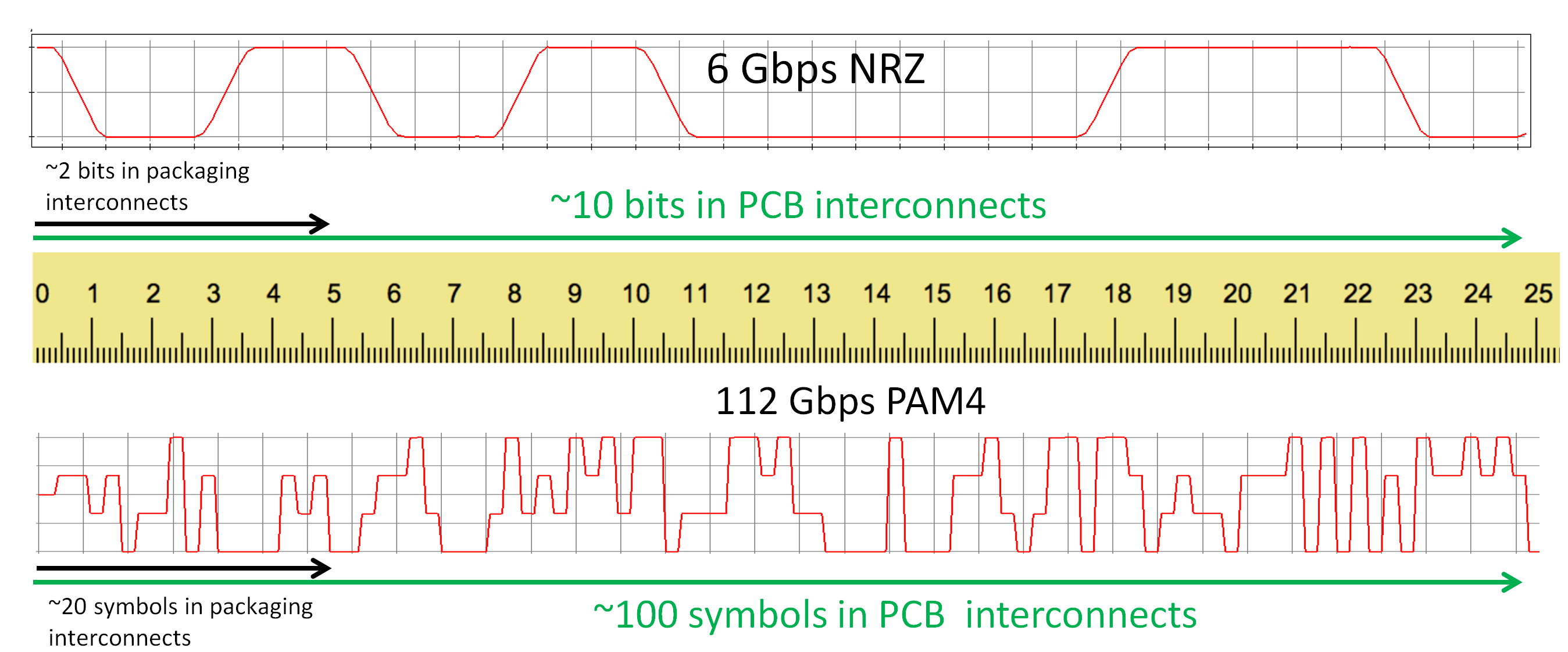
Figure 1: PCB and packaging interconnect scale in bits for 6 Gbps NRZ signal (top) and in symbols for112 Gbps PAM4 signal (bottom).
The ruler in Figure 1 provides a scale in cm. A slowdown factor of 2 is used for the illustration of the spatial spread in a typical PCB dielectric with Dk=4. We can see that at 6 Gbps NRZ, only a couple of bits are simultaneously in the packaging part of interconnects (about 5 cm or 2 inches) and about 10 bits are in the PCB part (about 25 cm or 10 inches) at the same time.
With the data rate increased to 112 Gbps and PAM4 modulation used, we can observe about 20 symbols (40 bits for NRZ) over the package section of interconnects and about 100 symbols (would be 200 bits for NRZ) in the PCB interconnects. The illustration in Figure 1 is for the ideal link, one without any kind of signal degradation. In real interconnects, the signals degrade. The degradation can be predicted with modeling or analysis or measured with scopes or vector network analyzers (VNAs).
Mathematically, it is easier to model the digital signal degradation in the frequency domain, assuming that the time domain signal is a superposition of harmonics. (Harmonics are just sinusoidal signals in time domain.) At this point, the analog problem in the time domain becomes the problem of harmonics in the frequency domain.
The first question always is: what is the bandwidth of the signal in the frequency domain and over what bandwidth should we have to model or measure it? To answer this question, we have to investigate to see what we would lose by neglecting the harmonics above the maximal bandwidth frequency.
Spectra and Bandwidth of High-Speed Data Signals
Let’s take a closer look at the power spectral density (PSD) of 6 Gbps NRZ signal with 50 ps rise time shown in Figure 2 for a pseudo-random bit stream PRBS7 (computed with Simbeor SDK).
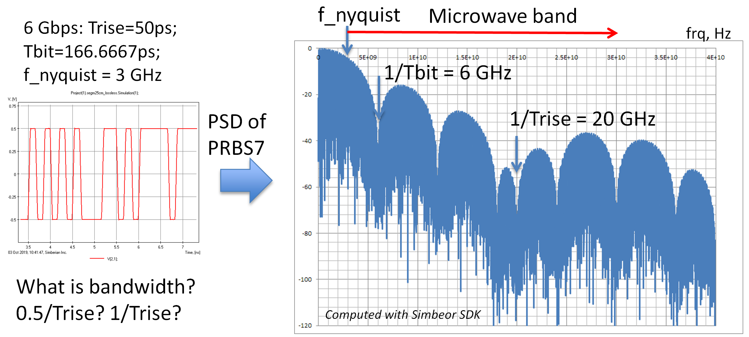
Figure 2: A fragment of 6 Gbps NRZ signal in time domain (left plot) and in frequency domain as the power spectral density in dB vs frequency (right plot).
We can see that the signal in the frequency domain is a superposition of harmonics with rapidly decreasing magnitudes. Starting from about 5 GHz, harmonic amplitudes are below -18 dB. The contribution of such harmonics cannot be ignored. The spectrum has a minimum at 1/Tbit (Tbit is the time for one bit or the unit interval) or 6 GHz, but rises after that up to -18 dB again.
The minimum bandwidth of a link to pass such a signal is defined by the Nyquist frequency (0.5/Tbit or 3 GHz in this case) [3]. As demonstrated in [1], accurate models or measurements must include the harmonics above the fundamental or Nyquist frequency. Otherwise the observed or computed signal in the time domain would be significantly distorted. This is because the power in the signal harmonics above the Nyquist frequency is significant, and it will define the signal shape or distortion if not properly accounted for.
Notice that most of the spectrum above the Nyquist frequency is in the microwave band! So, what should be the bandwidth for the modeling or measurement for such signals? Where should you stop the frequency sweep? Should it be 0.5/Trise or 1/Trise? At this point, we actually do not have enough data to answer that.
The real signal does not have a linear rise time as used for the spectrum evaluation above. It is not generated like that, and, even at the chip IO level, the signal is smoothed or filtered by the lossy and dispersive interconnects. The package may be very destructive too. So, for illustrative purposes, let’s take a look at the spectrum of the same signal after it passes through 50 cm (about 20 inch) of PCB stripline interconnect. The insertion loss of such a link is shown on the left graph in Figure 3 and corresponding response spectrum is shown in the middle graph below (40 GHz bandwidth):
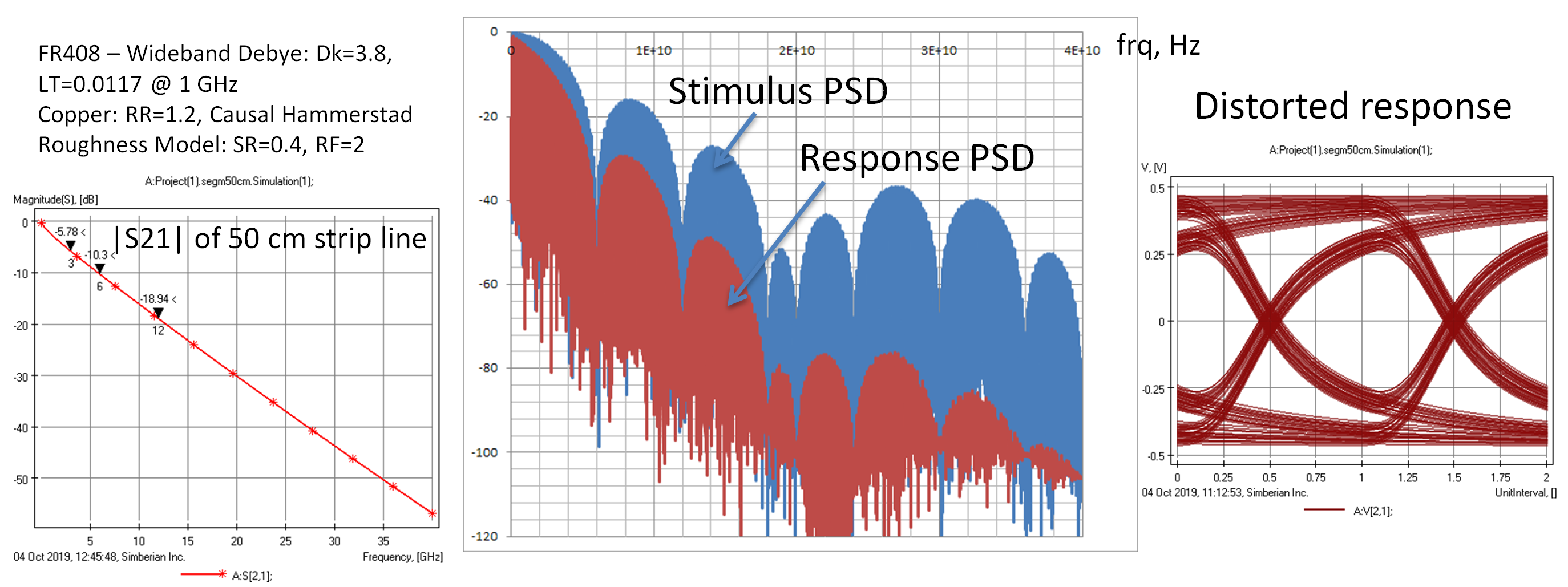
Figure 3: (left) The insertion loss of the sample link; (middle) the power spectral density (PSD) of the incident signal shown in blue (stimulus) and the PSD of the transmitted signal (response) shown in red; (right) the eye diagram (overlap of the pulses) shows the degradation of the ideal trapezoidal pulses.
Figure 3 shows that the rise time increases and there is deterministic (predictable) jitter due to the dispersion (it is actually not jitter, but usually called that). From the PSD plot we can see considerable attenuation of the high-frequency harmonics. If the analysis has to be done only for the transmission through the interconnect, it can be done with high accuracy over the same or even over a smaller bandwidth. Though, to define the bandwidth we need to quantify the errors introduced by the bandwidth deficiency. As shown next, this can be done with the analysis of single bit response.
The important point from this example is that an interconnect reduces the magnitude of the signal high frequency harmonics for better or worse, and it should be accounted for in the bandwidth identification.
Analysis of PAM4 Signals
Next, let’s take a look at the spectrum of a 112 Gbps PAM4 signal. The TX, with just 4 ps rise time (a little over-optimistic) is computed up to 500 GHz with Simbeor SDK and shown in Figure 4.
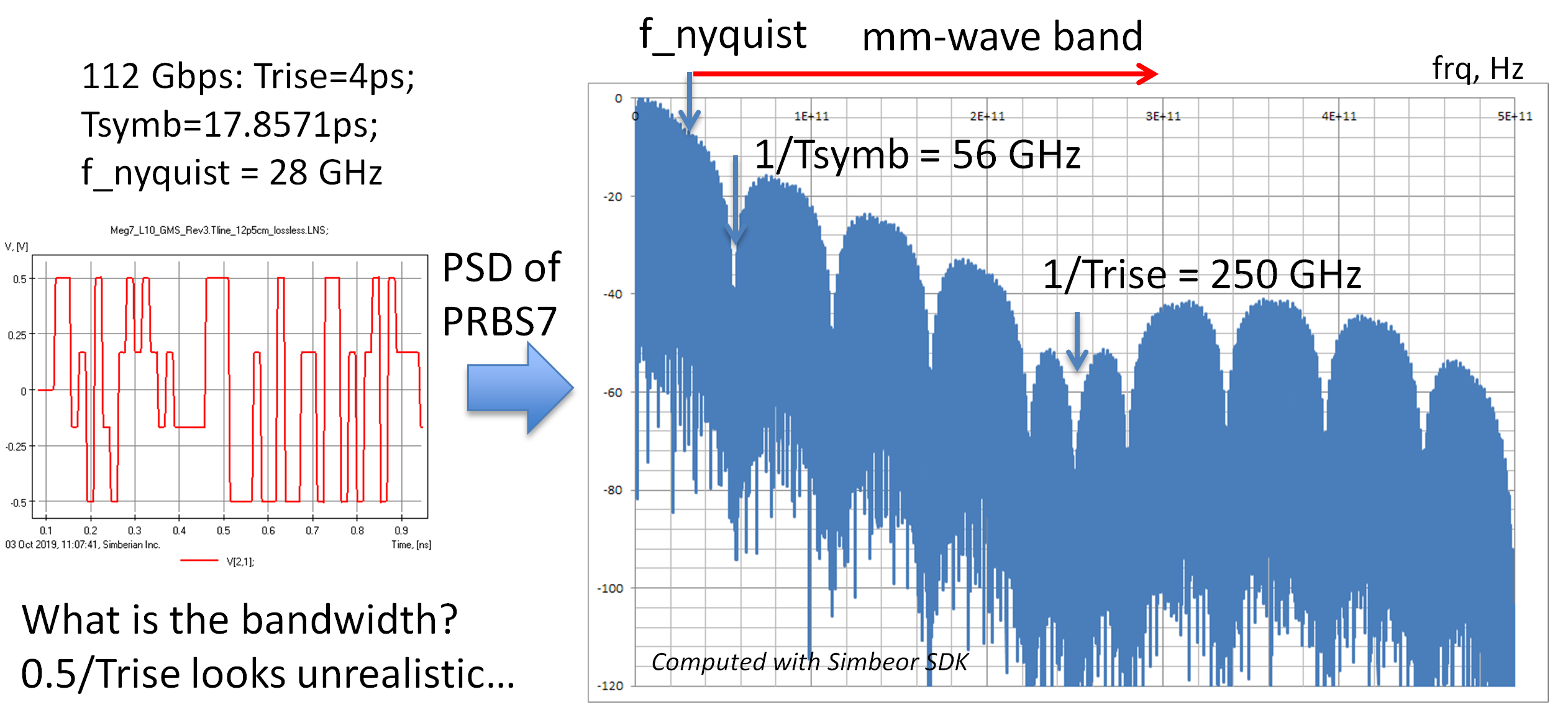
Figure 4: A fragment of 112 Gbps PAM4 signal in time domain (left plot) and in frequency domain as the power spectral density in dB vs frequency (right plot).
If the upper frequency estimate, 1/Trise, looked reasonable in the case of 6 Gbps (relatively easy to make models and measurements), it is completely unrealistic in this case. The Nyquist frequency = 0.5/Tsymb; it is 28 GHz in this case. The analysis or measurement up to this frequency will be highly insufficient as most of the signal power above this frequency will be unaccounted for. Notice that the signal spectrum above the Nyquist frequency in this case is in the millimeter-wave band (over 30 GHz).
Fortunately, the spectrum changes dramatically when the PRBS signal shown in Figure 4 on the left passes through 25 cm (about 10 inch) stripline interconnect as shown in Figure 5 (500 GHz bandwidth):
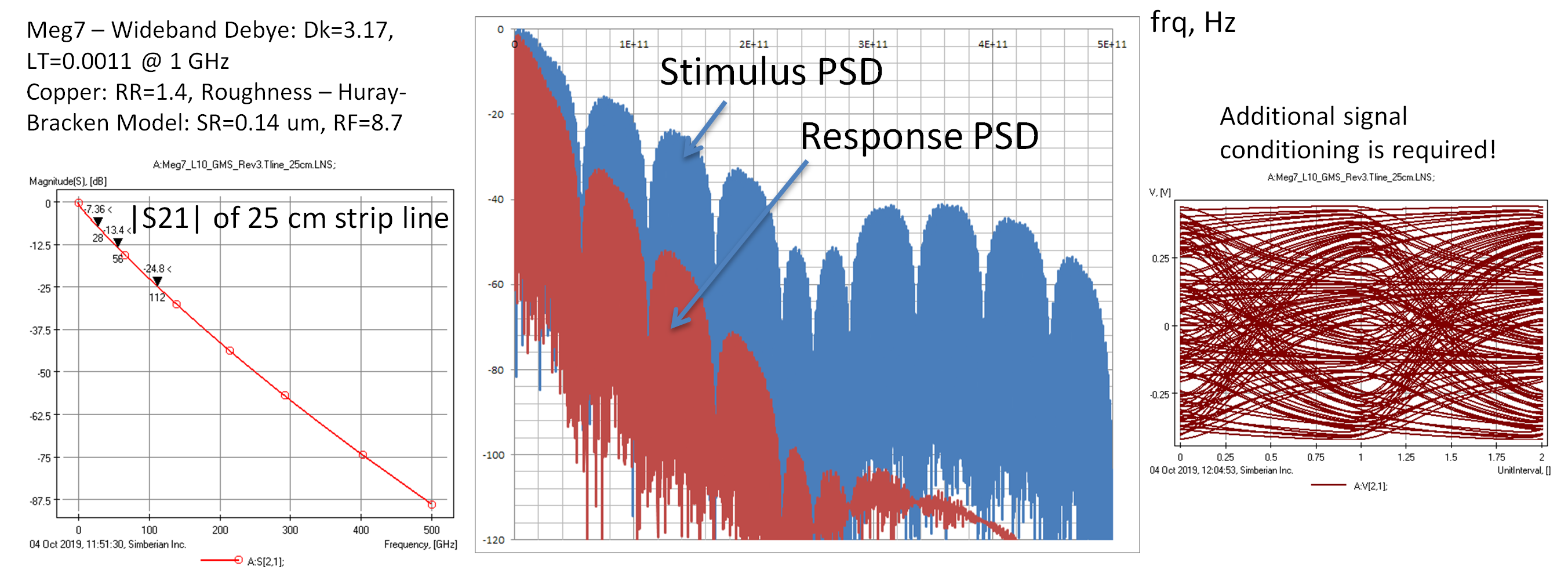
Figure 5: (left) The insertion loss of the sample link; (middle) the power spectral density (PSD) of the incident signal shown in blue (stimulus) and the PSD of the transmitted signal (response) shown in red; (right) the eye diagram (overlap of the pulses) shows the degradation of the ideal trapezoidal pulses.
Though, it is actually rather unfortunate, if you look at the eye diagram on the right – this is how a 112 Gbps PAM4 looks when it passes through the 25 cm of stripline on a typically designed PCB! It does not look good and requires additional signal conditioning to restore it.
So, what would be the bandwidth for 112 Gbps PAM4 signal? Should it be a multiple of Nyquist or fraction of the inverse rise time? We still need to evaluate the consequences of the bandwidth restriction. Technically, we have to evaluate the time domain signal distortion introduced by the spectrum harmonics above the bandwidth maximal frequency for a particular interconnect structure. As shown next, this can be done with the single symbol response.
Complications to the Spectral Analysis of Ultra High-Speed Signals
Here is what we have learned so far. The bandwidth required for modeling or measurements should be defined by the signal source spectrum (it may be computed or measured) taking into account the expected channel insertion loss (including all kinds of losses - absorption, reflections, leaks). The signal degradation reduces the power in high frequency harmonics and may reduce the required bandwidth as well. Though, such signal degradation and possible bandwidth reduction is unfortunate because it may degrade the signal up to the point of a complete link failure.
One more thing contributes to the bandwidth. We have not discussed possible coupling or crosstalk. The model bandwidth must be adjusted to account for the spectrum of the coupled signals that are not attenuated much at the near side (near-end crosstalk or NEXT, for instance).
Single Bit Response Numerical Experiments
There is a universal way to estimate the bandwidth with numerical experiments. Let’s give it a try. First, compute the single bit response (SBR) of a 6 Gbps NRZ signal passing through a 50 cm stripline link. We use a 40 GHz bandwidth as the benchmark and artificially restrict the modeling bandwidth to 3, 6, and 12 GHz and compare the SBRs as shown in Figure 6.
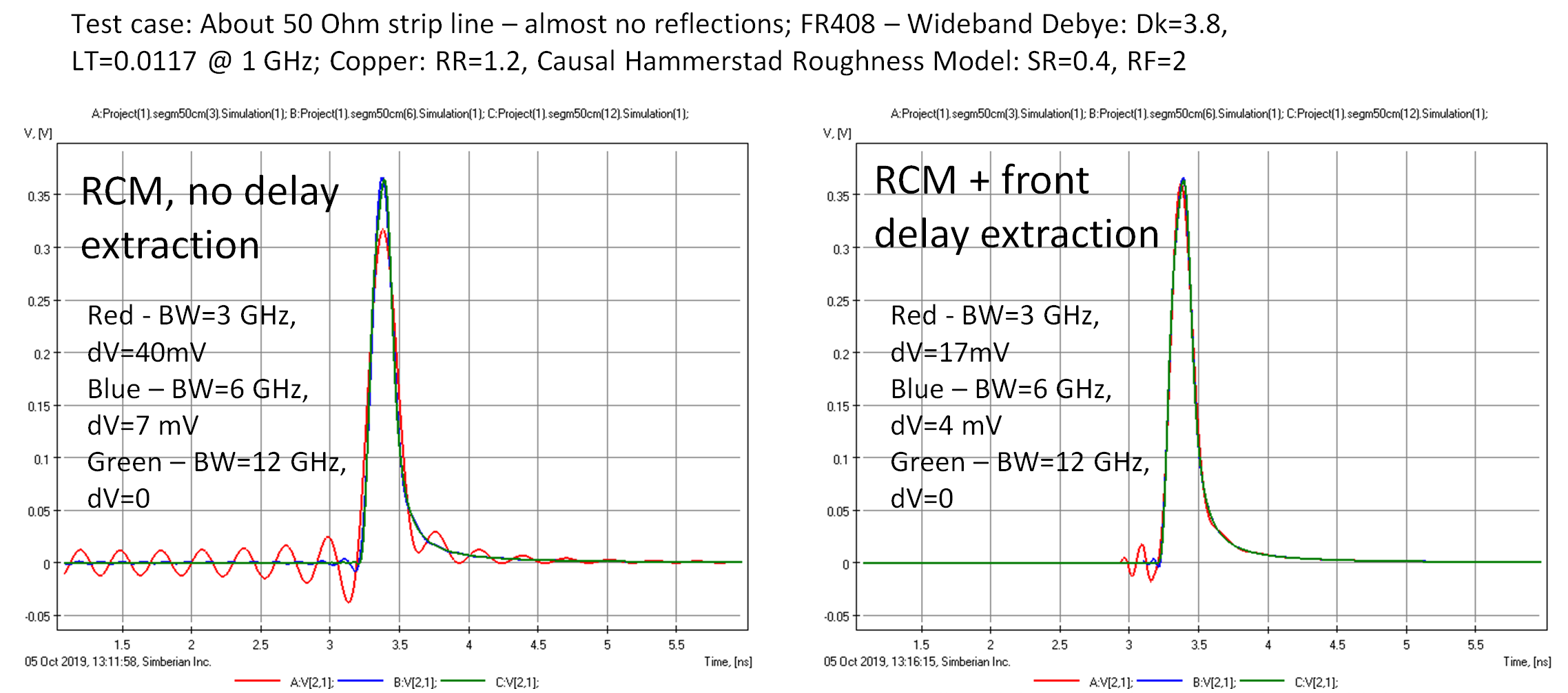
Figure 6: Single bit response (SBR) of a 50 cm stripline link for the 6 Gbps signal computed with different model bandwidths (BW) without the delay extraction (left plots) and with the delay extraction (right plots). dV is the error in SBR caused by the bandwidth deficiency.
The left plot in Figure 6 shows SBRs computed in Simbeor software with rational compact model (RCM) without the delay extraction. The RCMs are causal, but they approximate the original transmission parameter with high accuracy only up to the bandwidth maximal frequency (BW number on the plots above). The signal harmonics above that frequency are not delayed and attenuated by the RCM. The high-frequency harmonics appear as non-causal oscillations on the SBR (response comes before the expected time). We can see that if we restrict the bandwidth to just the Nyquist frequency, 3 GHz, the SBR will show non causality with peak-to-peak voltage noise of about 40 mV. That is over 10% of the benchmark SBR magnitude, computed with the sufficient bandwidth 40 GHz. That value may be considered as the error measure due to the insufficient bandwidth. In fact, the insufficient bandwidth usually shows up in time domain as oscillations or other defects caused by a mishandling of the high frequency harmonics. With the extension of the bandwidth up to 6 GHz (1/Tbit), the error is reduced to 7 mV, or about 2%, and the error is negligible with the bandwidth 12 GHz. That is what the model or measurement bandwidth should be for this case, ideally.
Obviously, one can reduce the “non-causality” by the delay extraction procedure. If the RCM is built with the frontal delay extraction, the error due to insufficient bandwidth drops as shown on the right of Figure 6. For the bandwidth 3 GHz, the delay in RCM corresponds to the signal frontal delay at 3 GHz. However, as we can see from the red curve on the right plot, the model delay is smaller than expected, and we can still see the oscillations caused by the high-frequency harmonics. Even if we somehow adjust the delay exactly to the value of the SBR delay, that will not save the day. The harmonics above 3 GHz will distort the SBR in some way. One possibility to avoid it is to predict the signal attenuation above 3 GHz. It may work for a simple transmission line segment, but it will not work for a link with discontinuities as discussed in the next example. So, the answer for the bandwidth evaluated with the model with the delay is still about 12 GHz; further increase of the bandwidth does not significantly change the SBR.
Will it work for another type of interconnect? Unfortunately, no. The numerical experiment should be repeated. Also, the result of such a numerical experiment will depend on the software used to compute the SBR. It is important to validate the software first. Capabilities of a particular software can be evaluated with a similar numerical experiment. Compute SBR for a set of models with different bandwidths and see if the response converges with the increase of bandwidth. If software uses DFFT, increase the number of frequency samples and see if the SBR converges when the number of samples increases. Also, compare the result to SBR computed with a different tool.
Single Symbol Response Numerical Experiments
Single symbol responses (SSR) for the 112 Gbps PAM4 signal discussed earlier and computed from S-parameters (shown on the left) measured for a 5 cm (about 2 inch) link are shown in Figure 7.
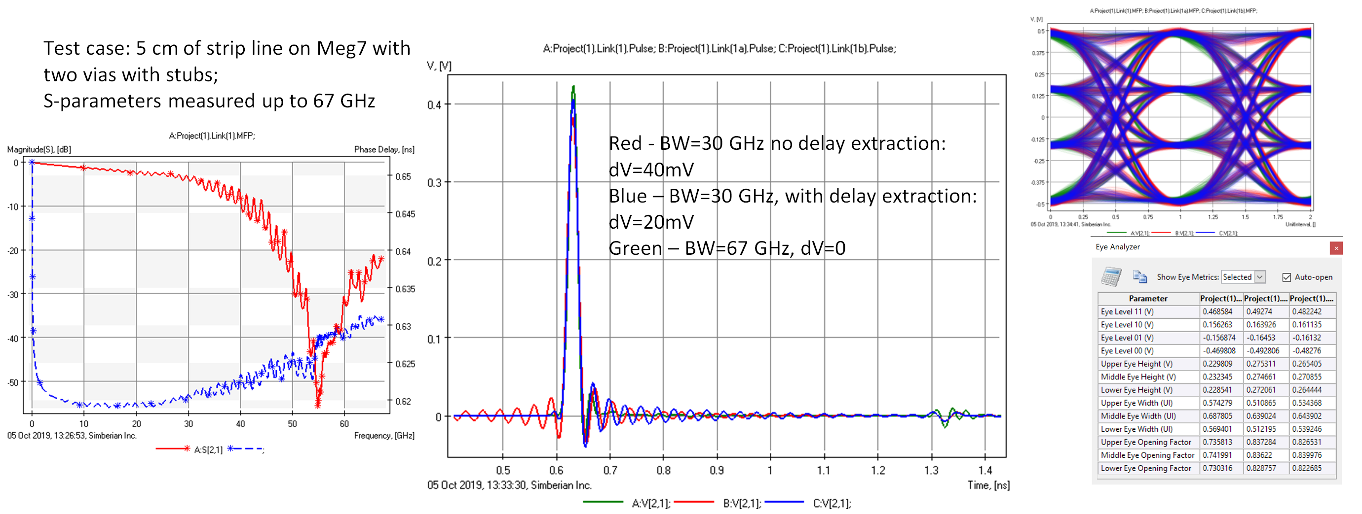
Figure 7: (left) Magnitude and phase delay of transmission parameter of a 5 cm stripline link; (middle) Single symbol responses (SSR) of the link computed with two different bandwidths (BW) and with and without the delay extraction (dV is the error in SSR caused by the bandwidth deficiency); (right) Eye diagrams computed with two different bandwidths (BW) and with and without the delay extraction.
In this case, a 67 GHz bandwidth is considered sufficient for SSR computation and used as the benchmark. It does not produce significant error (no visible non-causality in the SSR). That means that the power in the high frequency harmonics above 67 GHz is not significant for this structure. If the bandwidth is reduced to 30 GHz (a little over the Nyquist frequency), the error is about 40 mV out of 420 mV, or about 10%, for the model constructed with RCM and no delay extraction, and about 20 mV (about 5%) with the frontal delay extraction.
Note that the SSR pulse magnitude is closer to the expected magnitude with the delay extraction, but it is just a coincidence. The rest of the SSR is different from the benchmark case. The stub effect appears on all three SSR because the stub degrades not only the frequencies around the resonance at about 55 GHz, but also at the lower frequencies (visible as oscillations of the insertion loss on the left plot). The stub is a capacitive discontinuity at the frequencies below the first resonance. Though, the stub effect looks smaller on the SSR with the insufficient bandwidth.
The eye diagrams for all three cases may look very similar (they are shown on the right of Figure 7 with the eye measurements computed with Simbeor Eye Analyzer tool). The eye diagram may be not suitable for a bandwidth deficiency evaluation. The outcome of this numerical experiment is that we cannot reduce the bandwidth below 67 GHz for this structure. Most likely, we have to increase the bandwidth for interconnects with smaller reflections (no stubs) and with a smaller insertion loss. A numerical experiment should be the next step, to have a more definite answer.
Conclusion
This article demonstrates the importance of numerical experiments in making a decision on the bandwidth for PCB or packaging interconnect modeling and measurements. By building models with an excessive bandwidth (requires only realistic transmission line models) and observing the effect of the bandwidth reduction on the simulated response, we can identify the minimum bandwidth for the system investigation before the signal is excessively distorted.
REFERENCES
- C.R. Paul, Bandwidth of Digital Waveforms, EMC Society Newsletter, #223, 2009.
- R. Stephens, PAM4: For Better or Worse – Is PAM4 Worth the Hassle, SI Journal, Feb. 26, 2019.
- H. Nyquist, Certain Topics in Telegraph Transmission Theory, Transactions of the American Institute of Electrical Engineers, Volume: 47, Issue: 2, April 1928.