
In my high-speed design courses, I am often asked what the spots are all over the outer surface layers of some of the PCBs I pass around during the class. Figure 1 through 3 are examples of this. It is called thieving by the PCB fabrication industry.

Figure 1. A Printed Circuit Board with Large Thieving Dots Added to the Outside Layers
Notice that there are round dots in areas on the outer layers where there are no circuit features such as traces, vias, IC mounting pads or connectors.
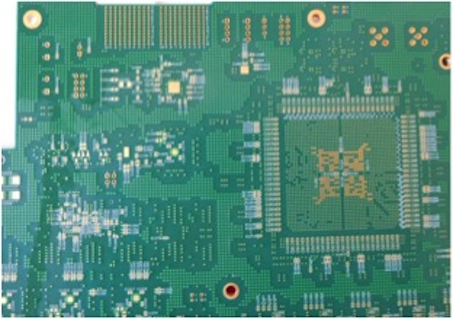
Figure 2. A Printed Circuit Board with Small Thieving Squares Added to the Outside Layers
In Figure 2 the small squares are added in the open areas of the surface between through holes and mounting pads of ICs, connectors and other components.
Figure 3. A Printed Circuit Board with Large Thieving Squares Added to the Outside Layers
In Figure 3 the added features on the outer layers are large squares.
A fair question is why are these added to outer layers? Why do they vary in size and who put them in the outer layer artwork? To understand this it would be good to review how outer layer plating is done.
Outer Layer Plating
Outer layer plating is done to deposit copper in the vias and component lead holes to form connections from one side of the PCB to the other and to make connections to signals and planes on inner layers. In order to provide a path for the plating current needed to plate the copper in the holes, the two outside layers of a PCB are kept solid copper until after drilling and plating.
Panel Plating
In the early days of PCB manufacturing, the entire panel on which a PCB is formed would be immersed in the plating bath after the holes had been drilled and cleaned of burs and debris. This is known as panel plating. The problem with panel plating is that copper is plated all over the surface even where there will be no traces or pads after final etching. This results in two undesirable side effects. The first is that etching of the unwanted copper has to go through the copper plated onto the outer surface as well as the original copper on the outer layer, using more chemicals and taking more time. The second is that as etching goes down through this copper it also etches sideways resulting in less accurate trace width control. To combat this set of problems a technique known as pattern plating was devised.
Pattern Plating
Pattern plating is a process that plates up copper on only the features that will remain behind after the outer layers are finally etched. These usually include all of the plated though holes, the traces and the component mounting pads. It is accomplished by applying a plating resist to the two outside layers after drilling has been completed. This plating resist is photosensitive and is exposed to a light that solidifies the resist in areas that are not to be plated. All of the unexposed resist is washed away, exposing the areas that must be plated. Then plating takes place.
The problem with pattern plating is that if the features on the outside layers are not evenly distributed across the surface, the plating currents will not be evenly distributed, as in the figures above, and some areas will plate more heavily than others, including vias and connector holes. When there is a need for very uniform plating, such as in the holes of a press fit connector, something must be done to spread the plating current evenly across the entire surface.
Thieving
Thieving is the addition of “dummy” pads across the surface that are plated along with the features designed onto the outer layers. Their purpose it to provide a uniform distribution of copper across the outer layers to make plating current more uniform and plating in the holes more uniform. These dummy pads are connected together along with all of the other features that will be plated by the outer layer copper laminated onto the PCB stackup. After plating, the copper between the dummy pads is etched away leaving them isolated from each other and other features on the surface layers.
Who Adds Thieving to Outer Layer Artwork?
Each fabricator has algorithms that examine the distribution of copper in the artwork as supplied by the customer. The manufacturing engineering staff at the fabricator will determine how much copper must be added to achieve uniform plating, and this extra copper is added in the form of dots or squares. As can be seen in the opening figures of this article, each fabricator has a different shape and size for the thieving features.
Cautions About Adding Thieving
If there are traces on the layers just below where thieving has been added, these traces may have their impedance adversely affected if thieving is applied over them. In order to insure this does not happen a note must be added to the fabrication drawing instructing whether thieving is allowed and where it is permitted. The following is one way to specify this on a fabrication drawing:

Consequences of Not Adding Thieving to Outer Layers
If thieving has not been added to the outer layer of PCBs that have an uneven distribution of features to be plated (such as controlled impedance traces, holes for press fit connectors, and component mounting pads), then the features that are isolated will plate up with far more copper than those that are densely packed.
The controlling parameter for plating outside layers of a PCB is to insure that there is adequate copper plated into the vias and component mounting holes to insure robust connections. In most cases, the most critical holes are those that will receive press fit pins of connectors. The control on these is usually +/- 2 mils or 0.05 mm. Platers will allow plating to go on until this specification has been met. Without thieving, most other features will be plated with excessive amounts of copper, sometimes so much that finished hole size is too small or trace impedance is thrown off.
Thieving is a method used by fabricators to insure more uniform plating of copper in the holes drilled through a PCB. It is necessary to insure that plating current is uniformly distributed over the outer layer surfaces of a PCB when the distribution of holes to be plated is not uniform, insuring uniform plating of copper. It is not required on inner layers as they are exposed only to etching and do not require plating.