
There are many questions about measuring Power Delivery Networks (PDN), but these two are very common ones. Why do we calibrate the 2-port measurement with a 1Ω shunt resistor and why do I use DC blockers on both ports? In this article I’ll provide responses to both of these questions. The measurement setup in Figure 1 is an example where I used both the 1Ω calibration and the inclusion of the DC blockers.
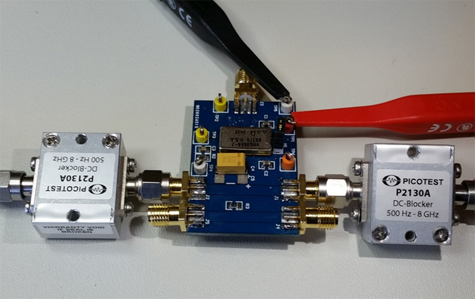
Figure 1. Voltage regulator test board with a pair of SMA connectors connected to the regulator output and a pair of SMA connectors connected to a 1Ω calibration resistor (R3) . (Image courtesy AEI Systems).
Why are DC blockers used on both ports?
The second question is easier to answer than the first, so let’s answer that one first. There are two reasons for the use of the DC blockers. First, the standard 2-port measurement connects both instrument ports (typically 50Ω) to the VRM being tested. These ports result in a load current of Vout/25 and this can be significant in comparison to the device loading. For example, measuring a 2.5V low power voltage regulator the port loading would add 100mA of output current. This 100mA can be more than the maximum load of the device, can overload the regulator and can greatly alter the regulator performance, which is load current dependent.
The DC blockers isolate the instrument from the voltage regulator module to eliminate such DC loading. A second reason for the inclusion of the DC blockers is to protect the instrument inputs from overvoltage. With that said there are a two points to be aware of. Wideband low frequency DC blockers are generally constructed using ceramic dielectric capacitors, which are DC voltage bias sensitive. The low frequency limit will increase with DC voltage applied. The graph in Figure 2shows the typical impact of DC bias on the P2130A wideband DC blockers along with a curve-fitted equation that can be used to estimate the low frequency limit. Always calibrate the setup with the DC blockers installed and beware of this DC bias effect on the low frequency limit. For lower frequency the J2130A may be a better choice with a range of 100Hz-1GHz.
A low frequency DC blocker can still allow a significant voltage transient when the regulator is powered up, so be certain that your instruments offer transient protection and power the regulator gradually if that is possible to minimize the transient energy.
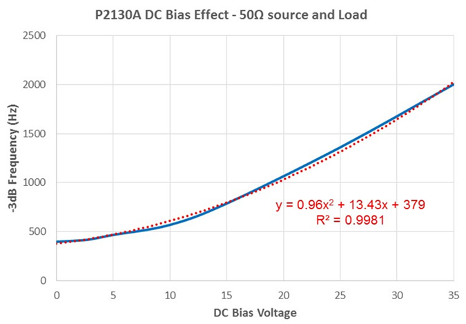
Figure 2. P2130A DC Blocker typical low frequency limit vs DC Bias voltage applied to the DC blocker
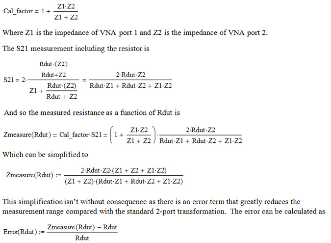
Why use a 1Ω shunt calibration?
A frequent question is why I calibrate using this unusual method. The test board shown in Figure 1 also includes two SMA connectors connected to a 1Ω shunt resistor (R3) for calibration of the 2-port measurement. There are several reasons I use this method.
For one, not every VNA includes the 2-port impedance transformation, and this includes the OMICRON Lab Bode 100 we use for our low frequency measurements. We could export the data and perform the transformation outside of the analyzer or we could use the automation interface to apply the transformation, but I like the simplicity of this method. I also like the minimal calibration hardware required. Rather than having to perform S-O-L on each port and a THRU calibration between ports, it is reduced to a single calibration.
The error is shown graphically in Figure 3 indicating that an error of +4% exists for resistance values below about 25mΩ and a -5% error is exists for resistance values above 2.37Ω. Despite the greatly reduced measurement range, the resulting range is quite usable in many applications. The resistance can be increased using a modified 2-port measurement [1]
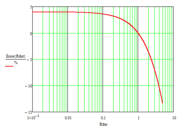
Figure 3 Measurement error as a function of the resistance being measured. The maximum error due to calibration is +4% and -5% corresponds to a resistance value of 2.37Ω.
Example measurements
In order to verify the measurement, several 2512 size resistors are mounted to circuit boards along with SMA connectors as shown in Figure 4. The 1Ω calibration resistor is connected in this setup picture. Three low value resistors, selected from the same vendor, are used to verify the measurement calibration.
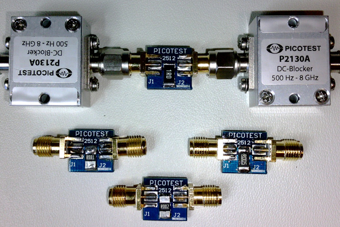
Figure 4. The VNA and DC blockers are shown connected to a 2512 size 1Ohm resistor. Similar resistance values of 1mΩ, 2mΩ and 5mΩ are shown in the foreground.
The pre and post calibration sweeps along with the measurement sweeps for 1 mΩ, 2 mΩ and 5 mΩ resistance values are shown in Figure 5.
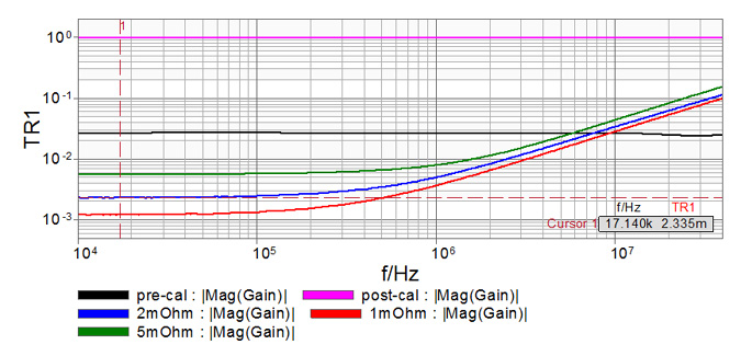
Figure 5. VNA measurement sweeps prior to calibration, after calibration and for the three low value resistors
The post calibration sweep is flat a 1Ω confirming the THRU calibration was performed and applied. The low frequency resistance values are reported as 1.2 mΩ, 2.3 mΩ and 5.6 mΩ while the corresponding inductance values are 420 pH, 500 pH and 660 pH respectively.
For comparison purposes, the resistors are measured using a 1 amp current source and a precision voltmeter as shown in Figure 6. This figure shows the results for the 1Ω calibration resistor.
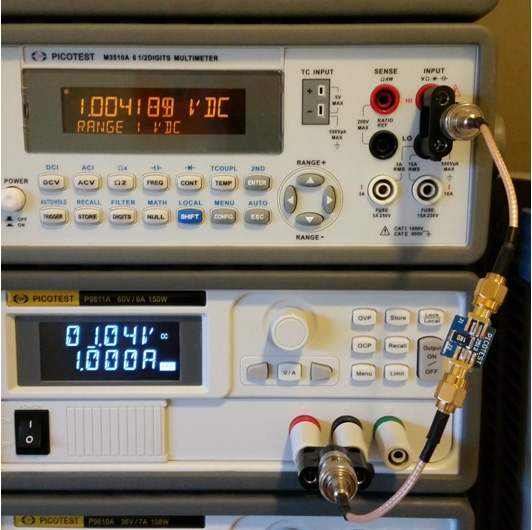
Figure 6. A power supply with current limit set to 1.00Amps is connected to one side of the resistor and a precision voltmeter is connected to the other side of the resistor. These connections replicate the connections used for the VNA measurements.
The DC measurements of the three resistors are 1.08 mΩ, 2.14 mΩ and 5.26 mΩ respectively. The VNA measurements are within 10% (1dB) for all three low value resistors using this simple 1Ω shunt calibration technique.