
Power rail measurements are important because they can identify potential sources of noise before they become a problem. However, measuring only the power rail noise at the board-level may be a misleading indication of the noise the die actually sees.
Best Practices for Power Integrity Measurements
Measuring a power rail on a board seems like a simple task. Like all measurements, it is easy to get a waveform on the oscilloscope’s screen, but it is difficult to have confidence you have eliminated the measurement artifacts and have a realistic measure of the actual signal present.
For example, the type of probe used to connect between the board/device under test (DUT) and the oscilloscope plays an important role. If you use a 10x probe, the tip loop inductance can act like an antenna and pick up RF noise either from the external environment, or from the near-field environment of the power rail itself. Figure 1 shows the voltage on a 3.3 V switch-mode power supply (SMPS) measured with a 10x probe, and the pick-up noise from an adjacent 10x probe shorted to itself, acting like an RF antenna.
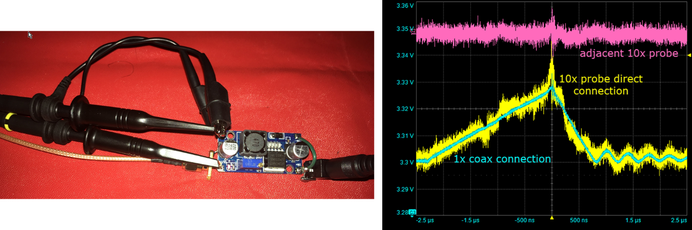
In this example, an independent measurement of the power rail voltage was made at the same location as the 10x probe using a coaxial connection on the board with a coax cable directly into the oscilloscope. This connection did not pick up any external or near-field radiated emissions, and it did not attenuate the signal by a factor of 10 like the 10x probe did. This is an example of the impact different probing methods can have.
A Simple Model for the PDN
Even with a good probing methodology, where you measure the power rail influences the noise you measure. It is important to always keep in mind that once the interconnects provide the correct connectivity, all they can do is add noise. Our job in designing the interconnects is to reduce the noise generated by the interconnects to an acceptable level.
In the power distribution path, the dominant parasitic introduced by the interconnects is inductance due to the loop inductance of the power and return conductors. The combination of the interconnect’s loop inductance and the discrete capacitors added to the power distribution network create embedded low-pass, LC filters.
Even though every conductor tied to the power rail is nominally the same net, the noise you would measure on different nodes of the power rail on the board will not be the same. What you measure depends on where the noise is measured. It depends on the victim; where the noise is generated, the aggressor; the frequency components of the noise; and the low-pass filters between the aggressor and the victim nodes.
Figure 2 is a simplified view of the PDN showing some of these low-pass filters.

Depending on the nature of the interconnects and the discrete decoupling capacitors, the pole frequency of the LC filters might range from a low of 10 kHz to a high of 10 MHz. For example, if the source of the noise is 50 kHz frequency components from the switching noise of the VRM, the higher frequency components may not be seen on the die, but some of the 50 kHz components may get through.
If the aggressor is the transient current from the die, the voltage noise on the die when depleting the on-die capacitance will drive dI/dt currents through the package lead inductance. While this noise will be measured on the die, since it generally has high frequency components, it will be filtered by the time it gets through the low-pass filters of the package lead inductance and board-level decoupling capacitors. It may not appear on a node on the board-level power rail.
To demonstrate this principle, I designed a simple board that creates on-die power rail noise from switching currents while allowing a direct measure of the on-die power rail voltage and the board-level power rail voltage. The circuit is just a simple clock that drives four of the inputs to a hex inverter chip. The other two pins of the hex inverter are used to measure the on-die voltages.
Measuring Rail Compression on the Die
In most applications, we do not have access to the bare die when the chip is assembled on the circuit board. If the IC package has not been instrumented with special pass-through features connecting the rails on the die to board pins, we have to rely on a special trick.
When the I/Os of a chip all share the same power and ground rails, which is often the case in small microcontroller devices, designated I/Os can be used as sense lines to measure externally the power rails on the die.
In digital CMOS outputs, the driver connects its output to either the Vdd or the Vss rails when its output is set to a HIGH or a LOW, respectively. This means that an I/O set as a HIGH or a LOW provides a direct connection to elsewhere on the board from which the Vdd or Vss rails can be measured, relative to the local ground on the board.
We call these special I/Os a quiet HIGH and a quiet LOW line. When they are set as a fixed value, their output voltage should not change. Any voltage variation on these lines is only due to noise either on the rail to which they connect or picked up somewhere along their signal-return paths. If these connections are designed as uniform transmission lines with a solid return plane, with other signals far away, the voltage measured at these test points will be dominated by the voltage of the on-die rail relative to the local board ground of the test point.
The equivalent circuit of a typical CMOS I/O showing the connection from the on-die rails and the board-level test points is shown in Figure 3.

All the measurements of the test points on the board are done as single-ended. This means the measured voltage is the voltage of the test point relative to the local ground location where the oscilloscope probe’s ground makes contact with the board ground plane.
The voltage measured at the Vdd test point is not actually the Vdd on the die. It is the Vdd on the die relative to the board ground. If there is ground bounce noise on the Vss rail, its voltage, and the entire chip’s Vss rail, may bounce relative to the local board ground. This bounces the Vdd rail the same amount, relative to the board ground.
What we really care about is the voltage rail on the die between the Vdd and Vss rails. This is Vdd – Vss, with each of them measured relative to the same board ground reference point. We sometimes refer to this value as rail compression. It is how the voltage rail on the die compresses due to currents switching.
What we actually measure is the voltage on the test point relative to the local board ground plane. As long as there is no additional noise picked up on the test lines from where they leave the package to where they reach the test point, the measured voltage difference between the Vss and Vdd test points would be equal to the rail compression on the die.
The process is then to measure the quiet HIGH and quiet LOW test points when other I/Os switch. When the oscilloscope is triggered by one of the I/Os switching, the rail compression can be measured from the Vdd and Vss quiet lines. The set up for this and the measured quiet HIGH and quiet LOW test points are shown in Figure 4. The rail compression can be displayed on the screen using an oscilloscope math function calculating Vdd – Vss.

In this example, the Vdd power rail was 3.3 V. The measured rail compression during the time at which the I/Os were switching was as much as 1.2 V. This is huge. It is so large that it affects the output signal rise time and would have caused false triggering on other I/O lines. If this rail was also used by the core logic, bit errors would definitely be generated.
On-die Rail Noise and Board-level Rail Noise
Using the quiet LOW and quiet HIGH sense lines gives a direct measure of the rail compression noise on the die itself. This is what is important, since it is this noise which will affect the correct functioning of the die and the impact from noise on false triggering.
But, suppose you had not instrumented the chip and did not know the voltage noise on the die itself. Suppose you only measured the voltage noise on the power rail on the board, relative to the local board ground. What would you see?
Also on this test board is a test point connected to the 3.3 V output of the LDO. At this point, we measure the voltage noise on the board. It is exactly the same net as the Vdd rail on the die, but it is located some distance away from the on-die test point, and on the other side of the low-pass filter from the source of the noise.
Figure 5 shows the board set up and the measured on-die rail compression and on-board voltage noise synchronous with the I/Os switching.

On the oscilloscope trace in this figure, the measured on-board 3.3 V rail is about 0.025 V, a very small amount of noise when the I/Os switch while there is 1.2 V of compression on the die. This is because the noise on the die, the aggressor signal, has to get through the low-pass filter composed of the package lead inductance and the local decoupling capacitors to get to the LDO, the victim location. The pole frequency of the low-pass filter is about 1 MHz in this board. Since the rise time of this noise is about 1 ns, its bandwidth is about 350 MHz. Very little of this noise gets through the 1 MHz low-pass filter.
If we had measured the voltage noise on the board and seen just 0.025 V amplitude noise, we would have concluded that the power rail noise was very low and insignificant, not to worry. In fact, the actual on-die compression was more than one-third the entire power rail, large enough to affect robust functioning of the chip.
Without this sort of on-die measurement, you would have no idea your product was so close to failure, until some customer ran it through some operation that was sensitive to this large of an on-die noise level. Without the diagnostic of knowing how large the on-die power rail noise was, finding the root cause of the problem would be as difficult as hunting a snipe.
Summary
If you use measurements of the noise on the board as an indication of the goodness of various design decisions, be careful you are not drawing false conclusions.
Implementing the technique of using a quiet HIGH and quiet LOW I/O pin is a simple way of opening up a small window onto what is happening with the power rail of your die.
For more information, watch these two free webinars by Prof. Eric Bogatin:
Practical On-die Power Integrity Measurements
Secrets To Successful Power Rail Measurements