Abstract
While not long ago systems had only several serial links, it’s now becoming common for systems to include hundreds – and even thousands – of such links. This paper describes the development and analysis of a large system with thousands of serial links. Due to the system’s size and complexity, the design team invested in a multi-year effort to build and qualify a virtual environment capable of both verifying connectivity and simulating any and all of the channels. Problematic channels with incomplete system-level connections, poor eye openings, or high BER are quickly identified. Performance limiters such as inherent discontinuities (and their associated resonances), and Tx/Rx equalization imbalance are found and examined in detail. The virtual system is also used to guide design choices such as layer stacking, via construction, back-drilling, and trace/connector impedances. Processes to optimize and select equalization choices are also described.
Author’s Biographies
Donald Telian is an independent Signal Integrity Consultant. Building on over 25 years of SI experience at Intel, Cadence, HP, and others, his recent focus has been on helping customers correctly implement today’s Multi-Gigabit serial links. He has published numerous works on this and other topics that are available at his website siguys.com. Donald is widely known as the SI designer of the PCI bus and the originator of IBIS modeling and has taught SI techniques to thousands of engineers in more than 15 countries.
Sergio Camerlo is an Engineering Director with Ericsson Silicon Valley (ESV), which he joined through the Redback Networks acquisition. His responsibilities include the Chassis/Backplane infrastructure design, PCB Layout Design, System and Board Power Design, Signal and Power Integrity. He also serves on the company Patent Committee and is a member of the ESV Systems and Technologies HW Technical Council. In his previous assignment, Sergio was VP, Systems Engineering at MetaRAM, a local startup, where he dealt with die stacking and 3D integration of memory. Before, Sergio spent close to a decade at Cisco Systems, where he served in different management capacities. Sergio has been awarded fourteen U.S. Patents on signal and power distribution, interconnects and packaging.
Michael Steinberger, Ph.D., Lead Architect for SiSoft, has over 30 years experience designing very high speed electronic circuits. Dr. Steinberger holds a Ph.D. from the University of Southern California and has been awarded 14 patents. He is currently responsible for the architecture of SiSoft's Quantum Channel Designer tool for high speed serial channel analysis. Before joining SiSoft, Dr. Steinberger led a group at Cray, Inc. performing SerDes design, high speed channel analysis, PCB design and custom RAM design.
Barry Katz, President and CTO for SiSoft, founded SiSoft in 1995. As CTO, Barry is responsible for leading the definition and development of SiSoft’s products. He has devoted much of his efforts at SiSoft to delivering a comprehensive design methodology, software tools, and expert consulting to solve the problems faced by designers of leading edge high-speed systems. He was the founding chairman of the IBIS Quality committee. Barry received an MSEE degree from Carnegie Mellon and a BSEE degree from the University of Florida.
Dr. Walter Katz, Chief Scientist for SiSoft, is a pioneer in the development of constraint driven printed circuit board routers. He developed SciCards, the first commercially successful auto-router. Dr. Katz founded Layout Concepts and sold routers through Cadence, Zuken, Daisix, Intergraph and Accel. More than 20,000 copies of his tools have been used worldwide. Dr. Katz developed the first signal integrity tools for a 17 MHz 32-bit minicomputer in the seventies. In 1991, IBM used his software to design a 1 GHz computer. Dr. Katz holds a PhD from the University of Rochester, a BS from Polytechnic Institute of Brooklyn and has been awarded 5 U.S. Patents.
1. Introduction
Pre-layout simulation has been demonstrated in [1] to explore the feasibility of proposed serial links as well as their sensitivity to system variables. While exhaustive analysis of link performance against manufacturing variations is performed in [1] in a pre-layout context, this paper illustrates the advantages of an efficient post-layout (albeit, pre-hardware) environment capable of analyzing thousands of serial links in a reasonable amount of time. Specific link-level advantages include the ability to: (a) confirm system-level connectivity, (b) balance and optimize equalization, (c) quantify design margin against performance targets, and (d) identify discontinuity-induced resonances not found by pre-layout analysis. The fact that there is typically no other way to perform these tasks further underscores the value of analyzing a virtual system as detailed herein; a capability commonly referred to as Virtual Prototype Analysis or “VPA”.
The vision of VPA is to provide the ability to quantify electrical-layer performance of any or all of thousands of system-level links in a reasonable amount of time, pre-hardware. The authors are part of a larger team that has invested in a multi-year effort to enable the capabilities described. While post-layout analysis is not a new concept in the field of Signal Integrity (SI), high-speed serial links have brought significant changes in the way SI analysis is performed. In addition to the ability to simulate millions of bits, identifying and removing resonances and balancing equalization at the system level are just some of the significant process steps introduced by serial links and enabled by VPA. Once assembled, the virtual system further enables the examination of performance gains against design options. Since parameters such as back-drilling, connector choice/impedance, via construction, and layer ordering can be easily adapted, the system-level improvement of these cost-sensitive choices can be quantified without time-consuming hardware fabrication cycles.
Innovations achieved in the past decade have enabled VPA to be applied to thousands of serial links. Necessary model formats and simulation techniques (both convolution-based and statistical) capable of resolving 10-12 Bit Error Rates (BERs) and smaller have been well-documented elsewhere [2-5]. Instead, this paper addresses a significant barrier to deploying serial link analysis in a post-layout context: the ability to rapidly solve and simulate Printed Circuit Board (PCB) vias with sufficient accuracy. As such, attention is given to detailing recent advances made in via modeling. Furthermore, as mainstream data rates push above 5 Gbps there is little eye opening left at both the Rx pin and die [6]. At these data rates it is imperative to model and measure signal performance after Rx equalization is applied, as is now required by the majority of 3rd generation serial standards [7].
This paper illustrates VPA using a system of approximately 30 large-scale PCBs interconnected through a backplane fabricated with over 50 metal layers containing thousands of serial links ranging in length from about 12” to 36”. While the scale of this system is large, the concepts presented can be deployed in any system utilizing advanced high-speed serial link technologies.
Though data rates will continue to increase throughout this decade, the dominant trend will be “the parallelization of serial interfaces”. Indeed, the presence of thousands of serial links in a single system suggests the need to significantly scale our serial link analysis in width rather than frequency. The concepts presented herein are consistent with this theme.
2. Enabling Technologies
Beyond basic serial link analysis capability, Virtual Prototype Analysis (VPA) of thousands of serial links at data rates beyond 5 Gbps has necessitated innovations detailed in this section. Specifically, these include:
- The ability to quantify signal performance after the application of Rx equalization
- Rapid generation and simulation of hundreds of via models with sufficient accuracy
- Expanded capacity, throughput, and data mining capabilities
2.1 Post-equalized Rx Signal Performance
The majority of 3rd generation serial standards verify serial link electrical performance (typically Tx, Channel, and Rx independently) at a location referred to as the “Rx Data Latch” or simply “Rx Latch” as shown in Figure 1. This change has been necessitated by the lack of an observable signal at the Rx pins and/or pad. Instead, modeled or “reference” Rx equalization is applied to the signal at the Rx pads to extract a signal with a measureable eye opening. Example standards now specifying reference Rx equalization (CTLE=Continuous Time Linear Equalizer and/or DFE=Decision Feedback Equalizer) include the higher data rate versions of SAS, USB, and many others [7].
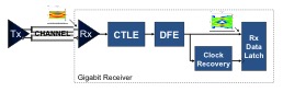
Figure 1: Typical Gigabit Receiver Showing Rx Latch
This methodology shift has brought about changes in both Test & Measurement (T&M) equipment as well as simulators and models. Essentially, it is now necessary for T&M equipment to include “simulators” capable of post-processing a waveform captured at a measurement location that can be probed (such as the Rx pin) [8]. Similarly, simulators now handle increasingly complex Rx models capable of modeling the performance of the signal after it is recovered by Rx equalization. Whether these are models of component behavior provided by a silicon vendor or modeled “reference” behavior provided by a tool or standard, they are increasingly available as executables in the AMI (Algorithmic Modeling Interface) format defined in the IBIS 5.0 specification [13].
2.2 Compact and Efficient Via Models
To support the comprehensive analysis of systems containing thousands of serial links, via modeling must satisfy three primary requirements:
- Computation of via models for many different via geometries must be practical.
- The via models must solve and simulate quickly.
- The via models must correlate to measured data.
The approach detailed herein is based on previously published papers that compare via models to measured data [9], [10]. Both papers conclude that vias behave like TEM transmission lines whose impedance can be calculated by assuming that there is a continuous shield at the edge of the antipad and running parallel to the via barrel (i.e., in the direction of the board thickness). [10] offered a motivation for this approximation by hypothesizing that radial TEM waves propagating from the edge of the antipad produced magnetic fields that approximately cancel the magnetic field from the via barrel. So far, this still appears to be a good approximation and explanation.
The via model deployed herein adds an equivalent circuit for the top and bottom pads and the exit trace to the transmission line described in [9] and [10]. This equivalent circuit is the combination of a few lumped and distributed elements, with element values derived primarily from physical properties. The model is accurate for single ended and common mode as well as differential mode. Since this equivalent circuit is relatively simple, it takes very little time to derive the model and compute its response.
[9] observed that the vias appeared to be longer electrically than one would have predicted based on the via length and the dielectric constant of the board. The explanation offered was that the effective dielectric constant for waves flowing in the direction of the board thickness was higher than that for waves flowing in the plane of the board. Further text can be found in [11].
To test the via length hypothesis advanced in [9], we extracted the insertion phase for the measured data for [10]. We also calculated the insertion phase predicted by our closed form model equations with the assumption that the dielectric constant is isotropic. Insertion phase is related to dielectric constant in that:
-
The dielectric constant determines the propagation velocity in the structure.

-
The group delay of the structure is the physical length of the structure divided by the propagation velocity.

-
The insertion phase is the integral of the group delay with respect to the angular frequency.

As shown in Figure 2 and the modeled and measured phase data from the Simple Via Experiment [10], the data supports the hypothesis of an isotropic dielectric constant rather than an anisotropic one because the dielectric constant determined from propagation in the X and Y directions is consistent with the delay in the Z direction.
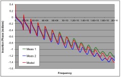
Figure 2: Modeled and Measured Phase from Simple Via Experiment
It therefore appears that a different hypothesis is required to explain the unexpected measured electrical length of vias. To create the via model used herein, we measured pad to pad S parameters for numerous differential traces on an unpopulated backplane. Each trace measured consisted of a differential via, a differential backplane trace, and another differential via.
The analysis approach was to convert the measured S parameters to Time Domain Reflectometry (TDR) plots and measure the electrical length of the via at the beginning of the trace in both single ended and differential modes. Since the measurement was made from pad to pad, the launching via was the very first element in the electrical path, so relatively precise measurements could be made. The measurement bandwidth was 20GHz, producing an effective TDR rise time of 17pS.
The measured electrical length vs. physical length is shown in Figure 3. In this Figure, the single ended measurements are shown using yellow symbols and the differential measurements are shown using red symbols. A line is extended through the measured differential values.
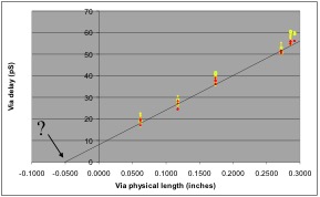
Figure 3: Bare Backplane Via Electrical Length vs. Physical Length
The line in Figure 3 was drawn through the differential mode data points because they show less spread than the single ended data points, and also because differential mode is not affected by the ground return impedance.
The slope of the line in Figure 3 corresponds to a dielectric constant of 3.61, compared to a dielectric constant of 3.41 for the traces on this particular PC board. This difference is within experimental error.
Figure 3 indicates that the increased length appears to be a constant length offset of about 0.05” rather than a decreased propagation velocity. This offset can be explained by considering the path the current must follow.
The via and trace depicted in Figure 4 consists of a top pad (typically at the top surface of the board), via barrel, bottom pad (typically at an internal routing layer), and exit trace (routing from the edge of the pad to the edge of the antipad).
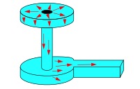
Figure 4: Via Current Flow
The current must follow the surface of the via structure, as depicted in Figure 4. For the structures we measured, the physical distances across the upper and lower surfaces of the top pad, across the upper surface of the bottom pad, and along the exit trace add up to 0.05”, the physical length shown as an offset in Figure 3. This is clearly a simplification of a complex set of electromagnetic field behaviors, but the data and physical reasoning support the hypothesis that the current paths across the top and bottom pads of a via measurably increase its electrical length. The resulting via model correlates well with measured data, making this approximation a useful one. Equally important, this via model can be calculated quickly and simulated efficiently, which are fundamental requirements of providing effective VPA.
Figure 5 and Figure 6 are representative examples of the model correlation obtained using post-route extraction with closed form equations and a via model that explicitly models the electrical length of the pad. The measured results from both ends of the trace (same vias on each end) are shown in blue and the model results are shown in red. In Figure 5, the time differences between the model and the measurements are much less than the 17pS rise time of the data, and the impedance differences are less than the impedance difference between the two ends of the trace (e.g., as measured at 400pS). Thus, the TDR data is well within experimental error. Similarly in Figure 6, the model matches the frequency domain ripples of the loss characteristic precisely and even at 20GHz the difference between model and measurement is less than 3dB.
The results shown are for a bare backplane (i.e., the fabricated PCB without connectors); however, the correlation is almost as good when connectors and cards are added.
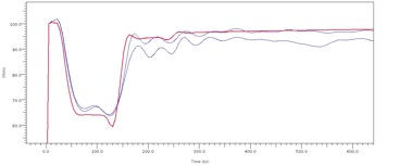
Figure 5: Typical Differential TDR Correlation Result
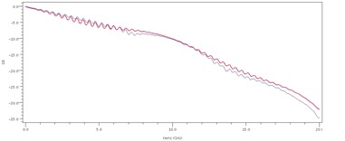
Figure 6: Typical Differential Insertion Loss Correlation Result
As demonstrated by Figures 5 and 6, this via model is more than adequate for analyses up to 10 Gbps, and provides useful results up to 20 Gbps. In the future, it could be improved by providing direct computation of the few remaining heuristic element values, and by explicitly calculating the coupling of vias to each other and to the ground plane cavity.
2.3 Capacity, Throughput, and Data Mining
Analyzing the behavior of a complete system requires that the VPA environment be able to process a fully populated virtual system model. This model may include dozens of PCB databases, totaling as many as 250,000 nets and 1,000,000 pins. A single post-route simulation run can require up to 25,000 simulations and generate 250,000 simulation files. The simulator’s analysis engine and database must scale to these levels and still provide reasonable performance.
Post-route simulations must be performed quickly enough to provide useful feedback to the PCB layout team. This means taking periodic PCB database revisions, performing simulations, interpreting results and providing updated physical design rules within 48 hours. Allowing a day for interpretation of results and updating design rules, that leaves a day for setting up and performing the post-route simulation run. The simulation tool must be able to extract post-route topologies automatically, generate via models on-the-fly, and construct connector models from slice data provided by the connector manufacturer. Given the size of the simulation task, turnaround time is reduced through the combination of Statistical modeling techniques (a Statistical simulation will run in seconds, while its Time-Domain equivalent may take 50-500x longer) and acceleration though parallel processing (server farms). The simulation environment must automate the process, since complexity is high and repeatability is key to ensuring quality, as VPA will be repeated many times throughout the course of the design.
Once the simulations are complete, it can be difficult to see “the forest for the trees”. It’s not enough to produce massive sets of raw simulation data, since the data needs to be analyzed and updated design rules created quickly. Productivity is increased when simulation output includes key performance metrics like eye height and width for each simulation case, associated with the physical characteristics of each channel. Organizing the results allows the designer to scan the data for best and worst case conditions, as well as overall trends and “outliers” that will require a more thorough investigation. There are two important aspects to post-route simulation data mining: automated reporting and interactive drill-down of results.
Automated reporting provides the first level of analysis and includes reports like:
- Electrical integrity checks: connectivity, polarity swizzles, Tx/Rx compatibility
- Physical characteristics: Net lengths, lengths by layer, potential resonant conditions
- Standards compliance: insertion loss, return loss, crosstalk ratio, eye mask pass/fail
- Performance metrics: Eye height, eye width, BER, optimized EQ settings
- Automatic identification of best/worst case cases and associated design variables
Once areas are identified for further investigation, problems are isolated by drilling down into individual simulation cases and performing what-if simulations to explore potential solutions. Important capabilities include:
- Correlate design metrics as a function of design variables or other performance metrics
- Correlate any waveform at any node in the network (including physically inaccessible nodes)
- Overlay compliance masks on simulation plots
- Edit post-route topologies to support interactive what-if analysis
Providing these capabilities in a way that provides reasonable turnaround with currently available computers is a tall order, but this is the problem that needs to be solved to enable full-system analysis.
3. Virtual Prototype Analysis
This section details system-level capabilities enabled by VPA that both verify interconnect integrity and optimize signal integrity.
3.1 Connectivity
The value of the virtual system’s ability to confirm system-level connectivity – or, interconnect integrity – can not be overstated. While schematic/PCB netlist forward and backward annotation capabilities ensure connectivity at a single PCB level, the virtual system confirms connectivity at the system level. Furthermore, as new PCBs are developed or existing PCBs are revised they are verified in the virtual system to confirm interconnect integrity and link performance prior to fabrication. In other words the virtual system can serve as a “test-bench” that verifies that new PCBs, perhaps developed by remotely located teams in different geographies and time zones, will perform as expected when plugged into the real backplane.
Interconnect integrity can be verified physically, electrically, and operationally, and examples of each method are provided below on a typical virtual system.
Physical connectivity for hundreds of differential pairs is confirmed in the Figure 7 which plots the combined driver to receiver length of signals spanning three PCBs (card, backplane, card). Thousands of signals are shown on the X axis versus each signal’s length on the Y axis in inches. The distribution of backplane net lengths is shown in red, and the corresponding total length of each pair is plotted in green. The fact that total length always exceeds backplane length provides the first level of confirmation that all signals connect from the Tx on one card across the backplane to the Rx on another card. Markers further quantify the distribution of PCB lengths, in this case revealing there are 518 nets with backplane lengths between 8” and 16”, 318 nets with lengths between 16” and 24”, and so on.
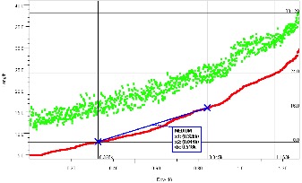
Figure 7: Physical Connectivity - Backplane and Total Net Lengths
While the data above suggests all nets are connected across the boards, we are only viewing their combined length. The plots in Figure 8 go one step further and show the differential insertion loss (left) and their associated fitted attenuation (right, an averaging of the insertion loss) of thousands of channels against typical industry masks in black. This confirms the nets are connected electrically, and demonstrates the range of system-level insertion loss we can expect to compensate for at various frequencies of operation.

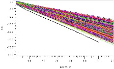
Figure 8: Electrical Connectivity – Insertion Loss and Fitted Attenuation
Plotting mask margins against channel loss in Figure 9 reveals that higher-loss channels slightly violate the mask (at very low frequencies, per the plot above right). In the plot below, red is insertion loss margin to mask and blue is the margin of the fitted attenuation to the mask.
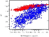
Figure 9: Insertion Loss and Fitted Attenuation Margins to Mask
With a good sense of electrical connectivity, we next examine operational connectivity by confirming that all nets produce an eye opening with typical equalization as shown in Figure 10 (eye height in red and width in blue). The eye openings recorded have a 10-12 probability of occurring, and hence are related to a certain BER as defined by the Rx characteristics.
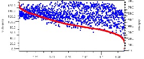
Figure 10: Operational Connectivity – 10-12 Eye Heights and Widths
As two of the channels show no eye height or width (extreme right Figure 10) it’s possible these channels are not operating or simulating correctly. Various methods shown below exist to build confidence that those nets are simulating and producing meaningful results. At left in Figure 11 we overlay hundreds of bathtub curves and confirm that two nets fail to yield an eye below a probability of 10-11 (highlighted in red), and hence show a closed eye at 10-12 probability in Figure 10. At right the statistical eye for these two nets confirms they do produce an eye at lower probability, yet - for reasons to be explained later - are less stable than the others.
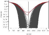
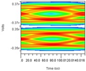
Figure 11: Operational Connectivity – Bathtub Plots and High BER Eyes
Additional operational connectivity tests include plotting all pulse responses in Figure 12 (at left) and eye parameters at 10-3 probability (at right, height in red, width in blue). The pulse responses reveal the range of channel delays and their corresponding attenuation, as well as a few nets with p/n reversal or “swizzle” (i.e., those nets with a negative-going pulse response). The 10-3 probability simulations demonstrate much wider eye openings than the 10-12 plot shown in Figure 10, which further confirms VPA is operationally functioning as expected.
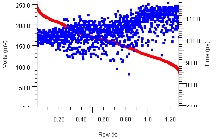
Figure 12: Operational Connectivity – Pulse Responses and 10-3 Eye Parameters
With connectivity and functionality confirmed, we are in position to extract design margins and resolve poorly performing channels prior to fabricating hardware.
3.2 Design Margins
The previous section has demonstrated that hundreds of thousands of datapoints have been generated for further examination during the design process. To illustrate this process, this section will focus on extracting and analyzing design margins measured on a cluster of links with medium length (around 20”) and moderate levels of equalization. Electrical performance will be judged by examining 10-12 eye heights and widths measured at the Rx die prior to equalization, while the gains of balancing system-level equalization will be addressed in a later section.
Figure 13 plots eye height on the Y axis versus eye width on the X axis for hundreds of differential pairs. The plot at left reveals that the majority of the signals cluster around 70mV/70pS eye height/width, yet a few of the signals have eye openings below 50mV/50pS. The plot at right presents the same data while delineating the direction of signal transmission into two different colors, red and blue. This plot reveals that, while many of the blue signals perform quite well, all of the signals below 50mV/50pS are transmitting in the blue direction.
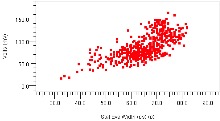
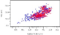
Figure 13: Eye Height vs. Eye Width, with Signal Direction
Recognizing that the worst eye heights also have the worst widths, the plots in Figure 14 allow us to study performance by plotting eye height on the X axis against system variables on the Y axis. The plot at left shows eye height versus backplane layer revealing that, in general, signals on deeper layers perform worse than those on upper layers. The plot at right shows eye height versus connector row, revealing that the worst performing signals utilize row 6 in the connector.

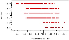
Figure 14: Eye Height vs. Backplane Layer and Connector Row
The data above allows us to hypothesize that the worst case nets in this length bundle are those with the following attributes:
- signals driven in the blue direction in Figure 13
- signals routed on the lowest (“deepest”) backplane layers
- signals connected through connector row 6
To test this hypothesis against signals with short, medium, and long backplane lengths in Figure 15 we plot all signal bundle eye height/widths below in blue and superimpose the subset of nets with these attributes in red. These plots confirm that nets with these characteristics describe the nets with the poorest performance.
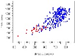
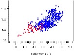
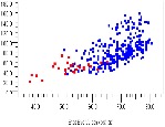
Figure 15: Channels with Least Margin Consistent Across Signal Lengths
Thus far we have demonstrated the value of extracting thousands of performance estimates for all signals in the system, and how these datapoints can be filtered to identify which signals perform poorly. The process shown illustrates the value of quantifying specific net-level performance across the system during a stage of development when design adjustments can be more easily made. The specific phenomenon identified above will be explained in more detail in the next section on discontinuity-induced resonance.
Link performance should also be plotted against both corner-case behaviors and decreasing BER, as shown in Figure 16. In this Figure, nine corners are created by combining three silicon corners with three interconnect corners as annotated above the graph. Eye heights are plotted at three different probabilities (implying three different BERs) delineated in red, green, and blue. This plot indicates that there is a significant change in design margin as we vary silicon and interconnect corners, as is evident by viewing any vertical slice in the Figure.
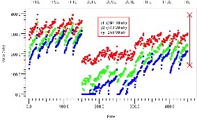
Figure 16: Corner Case Design Margins with Decreasing BER
3.3 Discontinuity-Induced Resonances
Using typical fabrication technologies, it’s not uncommon for the primary channel discontinuities to exist at component and connector locations due to their associated vias. Figure 17 shows a measured (red) and simulated (green) differential TDR plot of a typical (non-optimized) channel measured from the Tx to Rx. While much of the channel’s response is fairly flat around 100 Ohms impedance, the backplane connector locations are quite visible at ~1 nS and ~4 nS. Even though the impedance of the connector itself is roughly 100 Ohms, the connector vias create the two lower impedance dips on either side of the connector transition.

Figure 17: Measured (red) and Simulated (green) Channel TDR Showing Discontinuities
The presence of lower-impedance vias on both sides of the connectors cause a signal disturbance whose length is defined by the delay through the connector. The discontinuity causes some portion of the waves traveling through the connector to reflect off the 2nd via and return to their source. As the energy is reflected back, some portion reflects off the 1st via back into the connector, where again a portion will reflect back off the 2nd via and so on. This disturbance of defined length and the energy trapped in the structure can be referred to as a “discontinuity-induced resonance” or “standing wave”.
To better understand the discontinuities related to the connector vias, we must first quantify the delays through the various rows of the connectors. Placing a model of each row in the center of an ideal transmission line the Time Domain Transmission (TDT) plot in Figure 18 reveals the delays for each row, which are tabularized in Table 1.
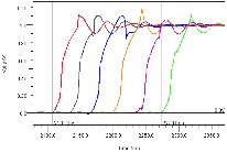
Figure 18: TDT of Connector Rows
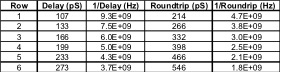
Table 1: Connector Row Delays
As Table 1 shows, the standing wave (or roundtrip) frequencies suggest all rows longer than row 3 are within the range of 6 Gbps frequencies. However this explanation is focused on the connector only, while the problematic discontinuities also include via structures on both sides of the connector. These vias must be included in the analysis, since they impose additional time delay as well.
A study of the various connector vias reveals that longest via delays are about 20pS on the cards and 60pS on the backplane. Combining these and counting half the via transit time to be within our problematic structure, in Table 2 we find that the row 6 delay is ~2 UI and hence energy from double-bit (and a portion of single-bit) patterns will resonate and degrade performance, as shown previously in the section on design margins.
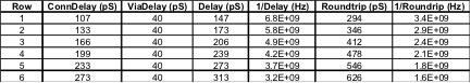
Table 2: Combined Connector and Via Delays
Further analysis shows that if a connector structure of this length is used it is helpful if at least one of the discontinuities on either side is removed. This lengthens the structure giving it more loss and therefore less pronounced standing waves. Solutions such as lower impedance traces and connectors and/or the use of specialized via structures can be used to smooth the discontinuities surrounding a connector. While pre-route analysis endeavors to exhaustively explore many connector/via combinations and other channel discontinuities, VPA has the potential to isolate combinations that may not have been comprehended previously prior to assembling the virtual prototype of the larger system.
3.4 System-level Equalization
While Tx equalization has been common since ~2 Gbps, the increasing presence of Rx equalization and models of the same enables system-level equalization optimization and balancing between the Tx and Rx. And, as this section will demonstrate, important performance gains can be realized by doing so.
Knowledge of the data stream enables a Tx to implement pre-cursor equalization, while an Rx can implement only post-cursor equalization. As such, we can hypothesize it would be best to let the Rx handle the post-cursor to preserve as much Tx amplitude swing as possible. Conversely, since the Tx is the only device capable of performing pre-cursor equalization, it should be tasked with handling pulse spreading during those bit times. The Tx may also be tasked with post-cursor equalization if the system requires more than the Rx can provide.
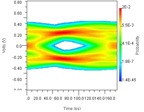
Using simulation to test this hypothesis, Figure 19 examines the performance of a typical net when sharing post-cursor equalization between the Tx and Rx. All eye openings are plotted at the Rx Latch with a small amount of Tx pre-cursor (-10%) and Rx CTLE applied. In the eye at left, the Tx has fully equalized the signal leaving little room for contribution from the Rx DFE. At center we evenly divide post-cursor equalization between the Tx (17%) and the Rx (18%). In this scenario the Rx eye is increased ~100mV suggesting that the extra energy delivered by the Tx is helpful. At right we see the eye shape when the Tx has only pre-cursor equalization and the Rx DFE’s post-cursor is at -32%. This scenario increases the eye height another 170mV at the Rx Latch, and the eye width has improved as well. From scenario 1 to 3, the eye opening has improved by 100% simply by deploying a system-level view of channel equalization.
Post: Tx=-35%, Rx=-2% Tx=-17%, Rx=-18% Tx=0%, Rx=-32%
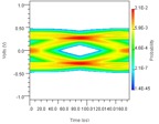
Eye: 248mV / 72pS 345mV / 73pS 513mV / 94pS
Figure 19: Eye Shape After Rx Equalization, Varying Post-Cursor Between Tx and Rx
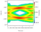
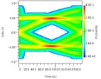
Though the eye openings above have increased substantially, this is at the expense of additional voltage swing (and hence power, noise, and crosstalk) in the system. The plots in Figure 20 reveal that, for the same three scenarios above, the pin-level performance has changed from over-equalized to under-equalized as expected. While the third scenario yields the best internal eye, it fails to deliver an acceptable eye at the pin. However, as newer serial link standards suggest, the relevance of pin-level eye performance continues to decrease.


Eye: 141mV / 60pS 150mV / 60pS 56mV / 21pS
Figure 20: Eye Shape Before Rx Equalization, Varying Post-Cursor Between Tx and Rx
The transfer functions for the three scenarios above are shown in Figure 21 against the unequalized transfer function in grey. While letting the Tx handle equalization (blue) successfully flattens the channel response, this is at the expense of reducing the low frequency amplitude. As such, less energy is delivered to the Rx for it to process and equalize. In green and red we see that allowing the Rx to assist in the equalization provides a more ideal response (~flat line at 0dB) up to the dashed vertical line. Green shows how sharing the post-cursor splits the difference in the low frequency response, yet the frequencies just below Fc are almost the same as when the Rx handles the post-cursor equalization (red). The pulse response of the four options is shown at right, using the same color scheme.
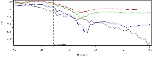
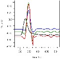
Figure 21: Transfer Functions and Pulse Responses Comparing Equalization Schemes
The plot in Figure 22 examines if the behaviors shown above are consistent across a larger number of nets. Eye heights for 50 nets using the three equalization options above are plotted using the same blue, green, and red colors. In this plot, grey represents the eye height at the die prior to equalization. The boxes at right quantify the band of eye heights for each of the equalization scenarios. While there is some overlap in the bands, the trend shown above is still true for this larger sampling of nets.
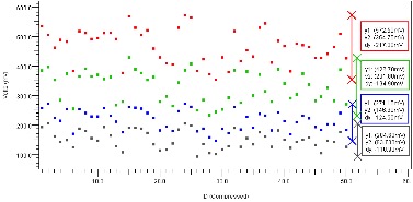
Figure 22: Eye Heights for 50 Nets Varying Equalization Schemes
Next we use VPA to examine the same three scenarios across thousands of nets in the system. As a result, over 20,000 eye shapes were derived and processed to 10-12 probability requiring ~20 hours on two CPUs. As such each simulation required about 3 seconds, or 6 seconds per CPU. An 8-CPU system could complete the task in less than 4 hours.
Figure 23 shows the results of these simulations. At left are the distributions of eye heights (red) and widths (blue) for each simulation scenario, and at right are the corresponding eye height/width scatter graphs. As all axes scales are the same (except the blue width values at top left), scenario 3 (Rx post-cursor) can be easily seen to perform the best.

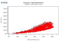
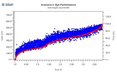
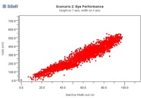
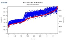
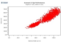
Figure 23: Eye Performance of Thousands of Channels, Varying Equalization Schemes
While system-level equalization tuning at a conceptual level is not new, the ability to deploy the tuning with sufficient accuracy on a net-by-net basis is one of the benefits of VPA. In addition to using VPA to explore pre-hardware design trade-offs (see next section below), equalization exploration and tuning can also assist with firmware updates in a post-hardware context.
4. Design Trade-offs
A virtual system enables comprehensive and rapid evaluation of design options that would be too expensive and time consuming to perform on physical hardware. Examples of items that can be easily modified and investigated using VPA include: PCB layer swaps, via back-drilling, back-drill stub length / number of depths, connector/route impedance variations, length variations and constraints, data rate, alternate PCBs, and complex via structures. A few of these trade-offs are illustrated in this section.
4.1 PCB Options
Since PCBs can be easily exchanged in the virtual system, it’s possible to use VPA to quantify which revision or performance option of a PCB is performing better. At left in Figure 24 we plot eye widths for Backplane_A on the Y axis versus eye widths for Backplane_B on the X axis. As there are more dots above the diagonal line we conclude that Backplane_A is performing better. At right is a similar comparison for plug-in card options, with Card_A on the Y axis shown to be performing better than Card_B on the X axis.
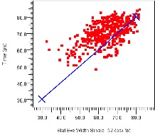
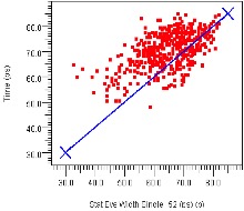
Figure 24: Eye Width vs. PCB Swapping, Backplane (left) and Plug-in Card (right)
As links are typically routed in a non-interleaved fashion for crosstalk mitigation, Tx and Rx signals tend to be on different routing layers. As such, we can also examine how performance changes when we swap signal layers (and hence transmission direction depth) within PCBs. In Figure 25 we examine eye heights for layer stacking options on a backplane at left and a plug-in card at right. In both plots signaling directions are represented by red and blue datapoints, and dots on the center diagonal imply performance is unchanged. Plots like this typically reveal that performance improves in one direction at the expense of a performance decrease in the other direction. In the Figure the blue/red performance change in the backplane (at left) are similar suggesting the layer swap is not helping overall, while on the card (at right) blue has gained more than red has lost suggesting that this swap is worth considering to improve overall system-level design margin.
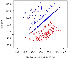
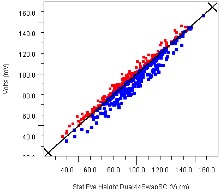
Figure 25: Eye Height vs. PCB Layer Swapping, Backplane (left) and Plug-in Card (right)
4.2 Via Back-drilling
While back-drilling is common on thicker backplanes, another design option easily quantified by VPA is the performance benefit that comes from also back-drilling vias on thinner plug-in cards. Figure 26 plots eye height (left) and width (right) changes with (X axis) and without (Y axis) back-drilling on the plug-in card. As such, all points below the diagonal indicate an improvement due to back-drilling. The plots below reveal that all signals either stay the same or improve – some times as much as 50%. Note that while signals received by the card (in red) improve with back-drilling, improvement is even more dramatic for signals transmitted from the card (blue). The plots reveal typically 20% improvement in margin on blue nets, yet more importantly improvement generally increases on signals with the least amount of margin.
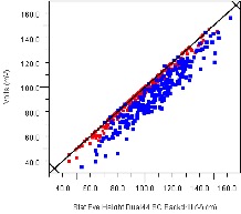
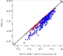
Figure 26: Eye Height and Width Variation When Back-drilling Plug-in Card
4.3 Data Rate
As architectural system-level throughput requirements change it’s common to assess how design margin changes with variation in data rate. Figure 27 reveals how eye height (left) and width (right) vary with an 8% decrease in data rate. Performance using the original data rate is on the X axis plotted against performance measured at the reduced data rate on the Y axis. As such points above the line indicate an improvement in performance/margin, which is shown by the markers to be typically 37mV in height and 10 pS in width which translates to ~30% increase in design margin for an 8% reduction in data rate.
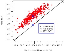
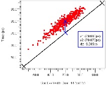
Figure 27: Eye Height and Width Improvements, 8% Data Rate Reduction
4.4 Impedance Changes
One way to alter discontinuities (and their related resonances) that limit performance is to change the impedance of nearby traces and connectors. Figure 28 plots how the eye height (red) and width (blue) changes in a channel limited by a discontinuity-induced resonance as we allow impedance variations in the dominant connectors and traces in the channel. Allowing four impedance options for traces on the backplane, both plug-in cards, and both connectors provides the 1,024 (210) permutations plotted on the X axis. From the plot we see that width tends to track height, and the eye opening can be improved up to 300%.
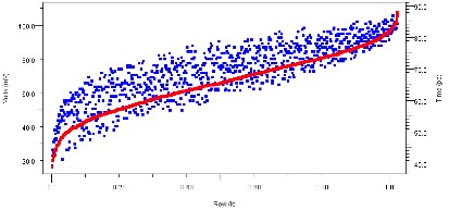
Figure 28: Eye Height and Width Variation vs. Connector/Trace Impedance Permutations
TDR plots of the original channel (lighter shades) and a channel with 300% eye improvement (in darker shades) are shown in Figure 29. Red is the direction of signal flow and blue shows the channel looking from Rx to Tx. Note that the impedance changes have not necessarily removed all the discontinuities, yet have certainly lengthened the distance between them.
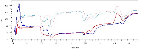
Figure 29: TDR of Marginal Channel Improved by Impedance Changes
5. Summary
In the coming decade, serial link analysis will be challenged not only by issues of frequency but also by issues of scale; trillions of bits will be processed across thousands of channels. While traditional SI methodologies had succeeded in moving post-route analysis to more of a verification step [12], this paper has demonstrated how VPA greatly assists serial link development in areas of system-level equalization tuning and design trade-offs. Furthermore, due to the thousands of channel permutations analyzed, VPA has potential to identify performance limitations caused by unexpected and/or unavoidable discontinuities that may have been overlooked by pre-route analysis. While challenges related to capacity, throughput, and accuracy must be solved to assemble an efficient virtual prototype system, this paper has demonstrated one approach taken and some of the benefits associated with overcoming these barriers.
Acknowledgements
The authors wish to thank Shashi Aluru, Minh Nguyen and Radu Talkad at Ericsson and Todd Westerhoff at SiSoft for their support. Many thanks to Jim Mangin and Steve Barbas for their support of this effort, and to John Lehman, Jose Paniagua and Brian Kirk at Amphenol-TCS for their continued help in advancing channel design and improving the connector footprint. Additional thanks to Orlando Bell at GigaTest Labs for consistently delivering high quality measured data. Without the efforts of these and other people this work would not have been possible.
References
[1] “Simulation Techniques for 6+ Gbps Serial Links” Telian, Camerlo, Kirk, DesignCon 2010 http://www.siguys.com/resources/2010_DesignCon_6GbpsSimTechniques_Paper.pdf
[2] “New Techniques for Designing and Analyzing Multi-GigaHertz Serial Links”, Telian, Wang, Maramis, Chung – DesignCon 2005,
http://www.siguys.com/resources/2005_DesignCon_New_MGH_Techniques_ISP_CA_PCIe_SATA.pdf
[3] “Introducing Channel Analysis for PCB Systems”, 2004 Webinar,
http://www.siguys.com/resources/2004_Webinar_Introducing_Channel_Analysis.pdf
[4] “New Serial Link Simulation Process, 6 Gbps SAS Case Study”, Telian, Larson, Ajmani, Dramstad, Hawes, DesignCon 2009 Paper Award,
http://www.siguys.com/resources/2009_DesignCon_6Gbps_Simulation_Paper.pdf
[5] “Adapting Signal Integrity Tools and Techniques for 6 Gbps and Beyond”, Telian
http://www.siguys.com/resources/2007_CDNLive_Adapting_SI_Tools_for_6Gbps+.pdf
[6] “Signals on Serial Links: Now you see ‘em, now you don’t.” DesignCon07 Article,
http://www.siguys.com/resources/2007_Article_SignalsOnSerialLinks.pdf
[7] SAS Specification, SAS-2, Project T10/1760-D, Rev 16, 18 April 2009, see also USB 3.0 etc.
[8] For example, see LeCroy 10/12/11 Webinar “USB 3.0 – Electrical Compliance Testing”
http://www.lecroy.com/support/techlib/webcasts.aspx?capid=106&mid=528&smid=663
[9] “Practical Analysis of Backplane Vias for 5 Gbps and Above”, E. Bogatin, L. Simonovich, C. Warwick and S. Gupta, paper 7-TA2, DesignCon2009, February 3, 2009.
[10] “A Simple Via Experiment”, Chong Ding, Divya Gopinath, Steve Scearce, Mike Steinberger, Doug White, paper 5-TP2, DesignCon2009, February 3, 2009.
[11] “Practical Design of Differential Vias”, Bogatin, Simonovich, Cao, PCD&F, July 7, 2010
http://pcdandf.com/cms/component/content/article/171-current-issue/7302-eric-bogatin-bert-simonovich-and-yazi-cao
[12] “An Optimized Design Methodology for High-Speed Design” DesignCon 2008
http://www.siguys.com/resources/1998_DesignCon_Optimized_SI_Methodology.pdf
[13] “Demonstration of SerDes Modeling using the Algorithmic Modeling Interface (AMI) Standard”, Steinberger, Westerhoff, White, paper 7-TA3, DesignCon 2008
Rev 1.1