
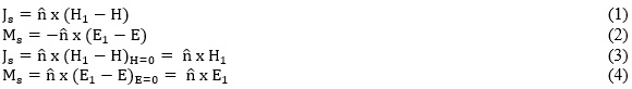
Huygens' boxes are used to identify and quantify the coupling path from noise to victim in portable electronic devices. The novelty of the proposed methodology is that multiple Huygens' boxes with different sizes are simultaneously defined on the same critical interface (e.g. USB, PCIe, MIPI) to find out the dominant contributor to the noise coupled to the antennas. The simulation reveals the underlying coupling mechanism, which in most of the cases is due to board-to-board connectors (BtoB), component , and regions with severe discontinuities. Conductive coupling is most critical and radiation coupling is kept to minimal values by employing conformal shield or metallic shied cans. The findings can be extended to most of the mobile devices due to repetitive interfaces and similar layout within the product design cycle.
Connected electronic devices, such as tablets, laptops, smartphones and the diverse ecosystem of Internet of Thing (IOT) products, include multiple RF systems. Radio frequency interference (RFI) or desense is a major concern in modern devices where multiple antennas and high-speed digital circuits co-exist.
RFI refers to the sensitivity degradation of RF receivers caused by interference within the same device. Typically antennas have a very high sensitivity, thus, the allowable levels (from -90dBm to -125dBm for various wireless standards) are much lower than the allowable emissions levels specified by the Federal Communications Commission (FCC). Therefore, having a device that is certified for FCC compliance does not necessary mean that the radio range is not limited by interference. When interference occurs it can lead to issues ranging from a dropped call (in the case of a mobile phone), to unlimited buffering while downloading a video, or even general malfunctions of the device.
Typically, RFI/desense problems can be divided into three parts: noise source, coupling path and victim (Figure 1). The coupling can be conductive (inductive and/or capacitive) and radiative.
The source (noise) is usually known by experience and in most of the cases it is related to switching mode power supply (SPMS) [1], high-speed interfaces (e.g. USB 3.0/3.1, DDR, PCIe), MIPI display and few more. The victim is well known and it is represented by the antenna/s, therefore, the most difficult part of the problem is the coupling path. So far, the coupling path is always treated like a black box represented by S-parameters [2] or field distribution (real or reconstructed [3]) and used to detect hot spots. Therefore, it is difficult to have any insights into the electromagnetic mechanism causing the coupling between noise source and victim.

The use of Huygens Box (HB) to define the noise source is not new and it has been treated by many works. However, it is believed that the Huygens' method can't guide the engineers on which part of the noise source causes the issue and how to fix it. In addition to this, the use of Huygens' boxes (HBs) has been always related to computing time reduction and/or the ability to keep proprietary information.
In this work, a new methodology that uses multiple HBs to identify and quantify the coupling path from noise to victim in portable electronic devices is proposed. HBs with different sizes are defined along the path of the same critical interface decomposing transmission line regions, discontinuity regions due to connectors, routing and components. It is found that most of the coupling path between the noise source and the victim is due to the use of connectors (BtoB) and/or severe discontinuities, such as component pads for passive filters. Furthermore, it is found that conductive noise is the critical part of coupling (since most of the chips are conformally or metallically shielded).
Huygens’ Principle and equivalence theorem
The technique to replace the noise source with a near field source (NFS) is based on the surface equivalence theorem, which states that a source in a volume can be substituted with its emitted fields (as the impressed sources) imprinted onto the surface that encloses this volume.
In Huygens’s equivalence principle, the actual sources are replaced by equivalent sources, and the equivalent sources produce the same fields as the actual sources within the region of interest. Figure 2 shows three cases for Huygens’s equivalence principle. By the surface equivalence theorem, the field outside an imaginary Huygens’s surface is obtained by putting equivalent surface electric and/or magnetic current over the surface.
The actual radiating source is denoted as current densities J1 and M1, as expressed by (1)-(2). The radiated fields are denoted as E1 and H1 in homogenous medium (Ɛ1 and µ1), n represents the unit normal vector pointing outward. In a similar way, the radiating source can be replaced by surface electric and magnetic current (Love’s equivalent Figure 2(b)), or by surface magnetic current with PEC filled inside (PEC equivalent Figure 2(c)), or by surface electric current with PMC filled inside (PMC equivalent Figure 2(d)), as expressed by (3)-(4).
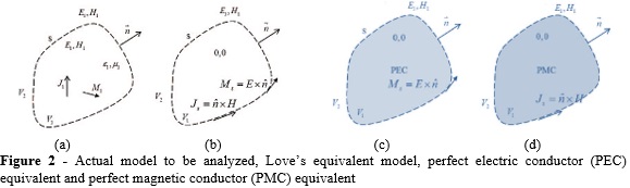
In this study, the surface electric current is calculated over the Huygens’s surface which is filled with perfect magnetic conductor (PMC). And for measurement convenience, the Huygens’s surface is chosen as a rectangular box. With the Huygens’s surface enclosing the radiating source, the fields outside the HB become uniquely determined by the equivalent source over the entire Huygens’s surface.
Validation of Huygens’s box principle
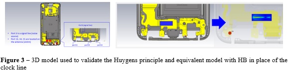
In order to validate the HB principle, we considered a real mobile device and define a clock line on the flexible PCB located on the bottom part of the phone and near the type-C connector (see Figure 3). Port 3 is placed on the clock/signal line (source) terminated with 50ohms resistor on the other side. Ports 13-14-15 are placed on the antenna (victim).
The results in Figure 4 show the comparison of the signal-to-antenna coupling for all the three ports between the original model and equivalent model, where the clock/signal line is replaced by the HB. Very good correlation is achieved in the 0-6GHz range of analysis. The small discrepancy in the very low frequency range is probably due to a truncation error which happens when the time signals are not completely decayed to zero. Figure 5 compares the H-field distribution at 800MHz for the original (full) model and equivalent HB model. Very comparable field distribution can be seen as a demonstration of the validity of the HB method in a real/complex structure.


Using multiple Huygens’ boxes
In [4] noise sources are quantified by using two Huygens boxes; however, besides the limitation on the total number of boxes (only two), they are used to characterize separate sources, thus separate coupling paths. Furthermore, two problems (named as forward and reserve) are used to predict the coupled voltage due to multiple noise sources. In our proposed methodology, multiple HBs are directly applied to the single noise source/possible coupling path and a single step is used to calculate the noise coupled to the victim, thus, possibly saving computational effort.
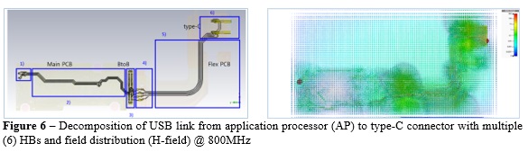
Figure 6 shows an example of a USB link from an application processor (AP) on a main board to a type-C connector on flexPCB. Six different HBs are identified in order to separate the contribution from the different regions, main PCB, BtoB connector, flexPCB with discontinuities regions, and type-C connector region. By analyzing the field distribution on the link, it is evident how most of the strength of the field is concentrated in the flexible printed circuit board (FPCB) region starting from the BtoB connector region (HB3).
A first test model consisting of a simplified mobile phone is considered for verification of the proposed methodology. A clock/signal line located on the top portion of the device nearby the antenna is considered. The line is excited by means of a discrete port on one side and loaded with a 50ohm resistor on the other side. A connector is placed on the line in order to study possible field variation and impact on the coupling mechanism to the antenna. Three HBs are defined as illustrated in Figure 7, where the comparison between the original model and the reconstructed coupling to the antenna (by mathematically adding the contribution of the three HBs) is also reported: if St is the coupling coefficient from clock/signal line to antenna, then St=SHB1+SHB2+SHB3, where HB1...3 are the HBs related to the three regions. Excellent correlation is verified over the considered frequency range 0-6GHz.
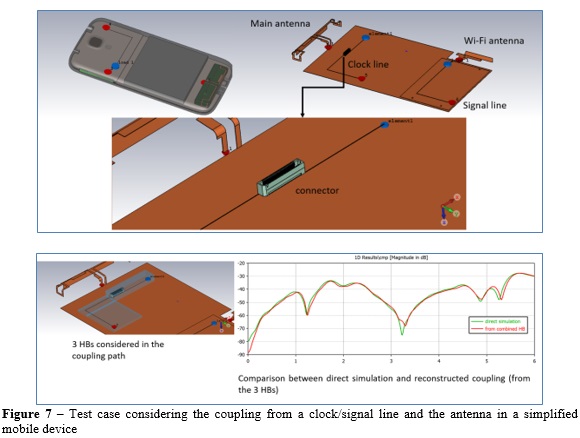
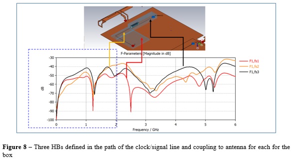
Figure 8 reports the contribution to the antenna coupling due to each HB. From these results, we can see how below 1.2GHz and within the frequency range 2.5-4.8GHz most of the noise coupled from the signal line to the antenna is coming from HB3, which is the HB including the BtoB connector. In the other frequency ranges, HB2 seems to be dominant, as one would expect due to the proximity of the signal line with the antenna and considering the fact that the reference is ideal in this test case.
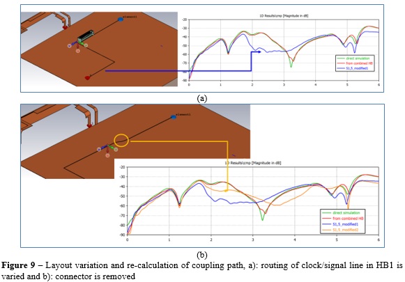
In practical cases, it is not possible to completely remove BtoB connectors, thus, we try to re-route the signal line according to the layout in Figure 9a by creating a 90 degree angle between the line reaching the connector and the connector itself. The main idea is to try to cancel out some of the coupled field between the signal line and the connector. The new coupling factor between signal line and antenna clearly shows improvements in the range 1.8-3GHz with more than 10dB reduction.
Just for reference, Figure 9b shows the results when the connector is completely removed. It is interesting to see that the coupled noise almost overlays to the previous case, showing a slightly lower reduction in coupled noise within the same frequency range. However the frequency range 3.5-4.5GHz is reduced by ~8-10dB with respect to the 90 degree signal line routing and/or original layout.
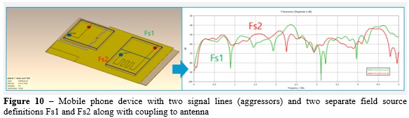
A meander shaped signal line is routed in Figure 10 on the same simplified phone model in order to analyze the different coupling mechanisms to the antenna. Fs1 and Fs2 are the two HBs defined in a way that Fs1 only includes a linear portion on the signal line, whereas Fs2 includes the meander line. The S-parameters coupled to the antenna are reported in the same Figure. In the low frequency range (< 1GHz) Fs1 and Fs2 generate very similar coupling values; however, there are consistent differences over the frequency range 1-5GHz and Fs2 is ~10dB higher from 1.5GHz to 2.5GHz. This finding hints to possible EMI degradation due to the presence of the meander line.
Case study 1
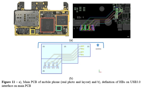
This test study consists of a main board used for a mobile device [5]. Figure 11 illustrates the board along with the two main ICs, the application processor (AP) and the memory, along with the routing of the USB 3.0 lines starting from the AP to the pads’ location of a BtoB connector. From here, a flexPCB brings the lines to the type-C connector, located at the bottom of the phone. The purpose of this study is to investigate the coupling mechanism between the USB lines and the diversity antenna, which is located on the top side of the device (victim port as represented in Figure 11).
For the sake of simplicity, four HBs are used to segment the area of interest with the intention of capturing the effects of the pads regions on the AP and BtoB side as well as possible radiation due to meander lines, which in some cases can generate common mode conversion and be detrimental for RF integrity.
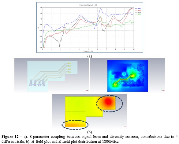
Figure 12a shows the coupling coefficients due to the HBs, and we can see how in the frequency range below 6GHz, the dominant factor of the coupling is represented by HB1, which is the Huygens box closer to the AP, but it also includes some discontinuities related to pads used for the placements of components.
HB4 is the second highest contribution to the coupling mechanism within the frequency range 0-2GHz. This is interesting since the position of HB4 is further away with respect to the victim point as compared to HB2 and HB3. However, HB4 includes a region of severe discontinuities as well as a BtoB connector. For f > 2GHz, HB2 and HB3 become dominant. Figure 12b confirms these findings with the H-field (A/m) distribution at 1800MHz on a cross section parallel to the signal lines. The E-field map related to the four HBs also show stronger coupling of HB1 and HB4.
Possible variations aimed to reduce the coupling to the antenna are: 1) moving the components further away from the AP, 2) re-route the portion of the lines in proximity of the BtoB connector and 3) (difficult to apply in the real product) completely remove the connector.
Case study 2
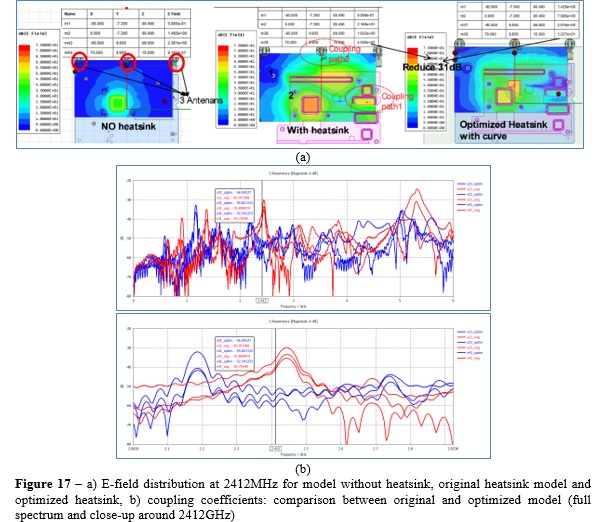
This test study analyzes a wireless router for first generation 5G (below 6GHz). Figure 13 shows a view of the router; note the large heatsink covering most of the bottom side of the PCB and three antennas symmetrically located on the top side part of the router. Total isotropic sensitivity (TIS) [6] measurements reveal problems for band 1 at 2412MHz (802.11b/g) with a value of about -71dBm, whereas it is within specifications for 5825MHz.
3D full wave simulation of the PCB with and without the heatsink when one of the PWR rails of the CPU is excited reveals that the coupling path with the antennas is mostly represented by the heatsink and both radiated and conductive paths exist (Figure 13a), although the conductive path is dominant.
Due to the long simulation time (> 1 day), it is not practical to use the real PCB to optimize the heatsink; therefore, a simplified model is generated. The PCB is modelled as a solid object, and the CPU is modelled as a metal patch which resonates at 5825MHz. The simplified model reveals the same coupling path as the original PCB. Figure 13b compares the electric field @ 2412MHz for the simplified model of the PCB + heatsink, and we can clearly see how the presence of the heatsink crates at least two coupling paths which cause degradation to the antennas.

In order to optimize the heatsink and reduce the RFI at 2412MHz, we first divided the region of the PCB model in 7 HBs with the goal of determining the area/s with dominant coupling to the antennas. The heatsink is mounted on the board, and it is electrically connected to the PCB frame by means of screws, as illustrated in Figure 14.
The only way for the current to close the loop and conductively couple to the antennas is through the metal screws; therefore, HBs are chosen in the surrounding regions. From the field distribution illustrated in Figure 13, it is also evident that the field excited by the patch (mimicking the IC) spreads in a radial way across the board. To break off such field propagation and reduce the radiated field coupled to the antennas, a slot/gap on the top of the heatsink is also required.
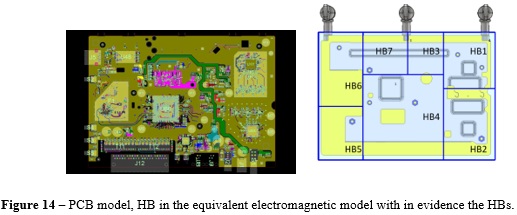
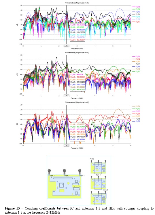
Figure 15 shows the coupling coefficients to the three antennas due to each HB showing the HB regions with dominant coupling. It is interesting to see that the coupling is not directly related to the geometrical distance; instead it seems more or less common for the three antennas, no matter which HB is considered as the excitation.
Also, the coupling coefficients between the HBs and the antennas and the dominant HB regions are in line with the field plot distribution illustrated in Figure 13 which shows how the antenna on the top left side is more immune to coupled noise as compared to the other two.
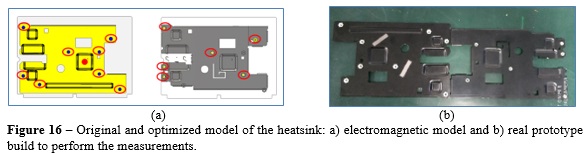
The dominant coupling between heatsink and antennas is due to HB3, HB4, HB7, and HB6. The goal is to optimize the heatsink by varying the position and the number of the screws and locating them in the HBs corresponding to higher field strength. After a couple of iterations, we came up with the optimized model showed in Figure 16, where the original heatsink geometry is also present for comparison purpose. The total # of screws is reduced from 8 to 6, new positions are provided, and in addition to this, a slot (whose length is exciting the frequency 2412MHz) is created in the region nearby the main IC to break down the radiated field.
The E-field distribution at 2412MHz for the optimized heatsink is illustrated in Figure 16, and the broadband coupling coefficient between heatsink and antenna are reported in Figure 17 where we can observe ~10dB field reduction from original to optimized heatsink. A prototype of the optimized heatsink was built and mounted on the wireless router, and the new value for TIS was reduced to -75dBm from the original -70dBm which is sufficient for antenna sensitivity. To further push the limits of the HB results and considering that some regions seems to be almost immune to conductive coupling to the antennas, a final simulation is performed by removing two of the screws located on the left side of the heatsink. This means that the total # of screws is reduced to 4 with consequent cost saving. The new results are illustrated in Figure 18, and it is possible to see how very similar performance (~ 10dB lower field strength at the frequency of interest) can be achieved as compared to the case with six screws.

Conclusions
A methodology to predict RFI/desense at the early design stage in mobile devices is introduced. The main idea is to use multiple HBs on the coupling path in order to detect the main contributor of the coupling to the victim (antenna), thus, making a change and minimize the RFI. Critical regions at set level can be identified, therefore, reducing the number of experiments aimed to analyze the signals to antenna coupling.
Two distinct test cases are used to benchmark the proposed methodology. The first one predicts the dominant coupling regions (components pads and BtoB connectors) in a mobile device when USB lines are considered as the aggressors. The second test case allows to design an optimized heatsink which helps to reduce the TIS of the upcoming 5G generation wireless router within the band 2412MHz (802.11b/g). The optimized heatsink not only provides good electrical performance, it is also more cost effective since up to four metal screws can be saved. In return this also allows larger routing space on the board.
An earlier version of this paper was presented at DesignCon 2019.
References
- K. Kim, H. Shim, A. Ciccomancini Scogna, C. Hwang,” SMPS Ringing noise modeling and mitigation for RFI solutions in mobile platforms”, IEEE Trans. On Components and Packaging, vol.8, n.4, 2018
- Y. Wang, S. Wu, J. Zhang et al, “A simulation-based coupling path characterization to facilitate desense design and debugging”, on Proc. of IEEE Int. Symposium on EMC+SIPI, August 2018, Long Beach, CA, USA
- J.Pan, H. Wang, Xu Gao, C. Hwang et al, “Radio Frequency Interference estimation using equivalent dipole moment models and decomposition based on reciprocity”, on IEEE Trans. on EMC, vol.58, n.1, 2016
- Y.Sun, B-Chyi Tseng, H.Lin and C. Hwang, “RFI noise source quantification based on reciprocity”, on proc. of IEEE Int. Symposium on EMC, August 2018, Long Beach, CA, USA.
- https://www.ifixit.com/Teardown/Huawei+P9+Teardown/62348
- A. Ciccomancini Scogna, et. al, “RFI receiver sensitivity analysis in mobile electronic devices'", DesignCon 2018 & Signal Integrity Journal.