


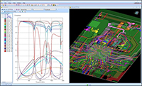
 The Cadence® Sigrity™ PowerSI® environment provides fast and accurate full-wave electrical analysis of leading-edge IC packages and PCBs to overcome increasingly challenging design issues such as simultaneous switching noise (SSN), signal coupling, problematic decoupling capacitor implementations, and design regions that are under or over target voltage levels.
 The Cadence® Allegro® Sigrity™ signal integrity (SI) integrated high-speed design and analysis environment streamlines creation of high-speed interconnect on digital PCB systems and IC packages. A range of capabilities—from basic to advanced—enable designers and electrical engineers to explore, optimize, and resolve issues related to electrical performance at all stages of the design cycle.
 The Cadence® Sigrity™ PowerDC™ environment provides fast and accurate DC analysis for IC packages and PCBs along with thermal analysis that also supports electrical and thermal co-simulation. Targeting both pre- and post-layout applications, the Sigrity PowerDC approach enables you to quickly identify IR drop, current density, and thermal issues that are among the leading field failure risks.
 Cadence® Sigrity™ PowerSI® 3D EM Extraction Option is three-dimensional (3D) full-wave and quasi-static electromagnetic field (EM) solver technology tailored for IC package and PCB design’s S-parameter model extraction for power-integrity (PI) and signal-integrity (SI) analysis. The adaptive finite element mesh (FEM) refinement technology provides consistent accuracy for complicated 3D structures.
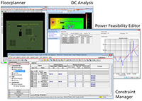 The Cadence® Allegro® Sigrity™ PI design and analysis environment streamlines the creation of power delivery networks (PDNs) on high-speed and high-current PCB systems and IC packages. A range of capabilities enable you to explore, optimize, and resolve issues related to electrical performance at all stages of the design cycle. The solution integrates tightly with Cadence PCB and IC package layout editors.
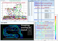 Uniquely equipped to let you perform a broad range of signal- and power-integrity studies in a single step, Cadence® Sigrity™ SPEED2000™ technology is a layout-based time-domain simulation tool for IC package and/or board design. Sigrity SPEED2000 technology combines circuit and transmission-line simulations with a fast, special-purpose full-wave electromagnetic field solver.
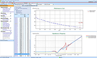 To ensure you get high performance at a system and component level, while at the same time saving between 15% and 50% in decoupling capacitor (decap) costs, Cadence® Sigrity™ OptimizePI™ technology does a complete AC frequency analysis of boards and IC packages. Supporting both pre- and post-layout studies, it quickly pinpoints the best decap selections and placement locations to meet your power-delivery network (PDN) needs.
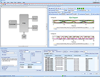 Cadence® Sigrity™ SystemSI™ signal integrity (SI) solutions provide a comprehensive and flexible SI analysis environment for accurately assessing high-speed, chip-to-chip system designs. The solutions support industry-standard model formats and automatically connect the models.
  The Cadence® Sigrity™ XtractIM™ tool provides a complete model extraction environment focused specifically on IC package applications. The tool generates electrical models of IC packages in IBIS or SPICE circuit netlist format. These concise parasitic models can be per pin/net RLC list, coupled matrices, or Pi/T SPICE sub-circuits.
 To keep up with the rapid advances in high-speed interfaces, you need to be able to run accurate, full-bus simulations in hours, instead of days. By converting models from transistor to power-aware IBIS behavioral, Cadence® Sigrity™ Transistor-to-Behavioral Model Conversion (T2B™) can help you meet ever-shorter deadlines by avoiding time-consuming transistor-level simulation and inaccurate non-power-aware IBIS model simulation.
 Cadence® Sigrity™ Broadband SPICE™ technology accurately and quickly converts N-port passive-network parameters such as scattering, impedance, or admittance (S, Z, or Y) into SPICE-equivalent circuits that can be used in time-domain simulations.
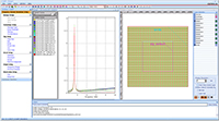 Cadence® Sigrity™ XcitePI™ Extraction technology takes chip layout data in GDSII or LEF/DEF formats, and generates a comprehensive SPICE model that consists of a fully distributed PDN and I/O nets and accounts for all electromagnetic coupling effects between signals, power, and ground.
 Please complete this form with the specific products, quantities and deliver requirements.
Company Profile
Cadence is a leading provider of EDA and semiconductor IP. Our custom/analog tools help engineers design the transistors, standard cells, and IP blocks that make up SoCs. Our digital tools automate the design and verification of giga-scale, giga-hertz SoCs at the latest semiconductor processing nodes. Our IC packaging and PCB tools permit the design of complete boards and subsystems.
Cadence also offers a growing portfolio of design IP and verification IP for memories, interface protocols, analog/mixed-signal components, and specialized processors. And reaching up to the systems level, Cadence offers an integrated suite of hardware/software co-development platforms. In short, Cadence® technology helps customers build great products that connect the world.
Cadence is headquartered in San Jose, Calif., with sales offices, design centers and research facilities around the world to serve the global electronics industry. More information about the company, its products and its services is available at www.cadence.com.
Contact Information:
Phone: 408-943-1234
Email: Click here to see email.
Website: http://www.cadence.com
Location:
Cadence Design Systems, Inc.
2655 Feely Avenue
San Jose CA 95134
United States