
The voltage regulator module (VRM) contributes system level noise in several ways. Power integrity (PI) engineers tend to focus on transient voltage noise related to high-speed dynamic current. Many PI simulators ignore the VRM noise and use an ideal resistor and inductor model to represent the VRM. This overly simplistic approach misses many potential system level issues.
Consider the simplest VRM model as a “black box” with one input and one output. This simplistic VRM contains six parameters for characterization:
1. Input self-impedance: predominantly negative resistance for a switching regulator.
2. Output self-impedance: generally used for target impedance assessment.
3. Input to output transfer: input voltage to output voltage transmission; power supply rejection ratio, PSRR.
4. Reverse transfer: output current to input current transmission.
5. Input noise current: predominantly switching induced.
6. Output noise: predominantly switching induced.
Each of these characteristics interacts with the system it is placed in and is therefore essential to predict and/or optimize the performance in the system.
In many higher current applications, the VRM also includes a SENSE input. The SENSE input is used to regulate the VRM output voltage at a specific location on the PCB, usually close to the load, in order to optimize the PI performance. This sense input adds another characterization parameter, providing access for measurement of the control loop. Simple representations are shown in Figure 1.

We can use a VPT SVGA0510S Hi-Rel hybrid DC-DC converter to illustrate the interaction between external system characteristics and internal VRM characteristics.
This converter, chosen for convenience, accepts a 5 VDC intermediate input voltage and provides a selectable 0.8 to 3.3 V/10 A output. The voltage is selected using an external “trim” pin and the 47.5 kOhm resistor sets the output voltage at 1.2 V. An accurate, validated simulation model of the converter offers the simplest, most efficient path to optimization and is used to show the interactions of the converter and the system. This model was created solely from external measurements using my published Measurement Based VRM modeling technique.
The simulation model provides two outputs. One output is a large- and small-signal state space averaged output. The other output is a harmonic balance output, providing spectral content and a high-fidelity replication of the large signal output ripple voltage. The converter, and the model, include a remote sense pin, so that the control loop can also be assessed. The simplified schematic of the simulation model is shown in Figure 2.

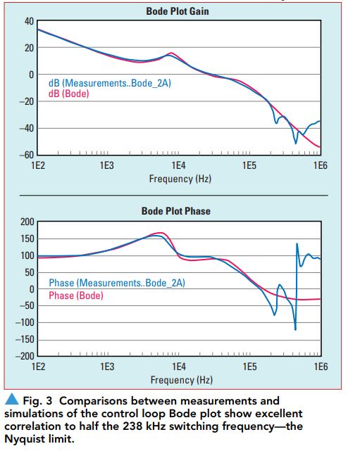
Before using a model for simulation, it must be fully correlated with measured data. While this example model is fully correlated, including the complete correlation would require much more space than a short article allows. Representative comparisons between the measurements and the simulations of the control loop Bode plots are shown in Figure 3.
In order to show the interaction between the VRM and the system, three system level variables are individually swept. An input filter inductor with a parallel 1 Ohm resistor is used to simulate an input EMI filter, an additional ceramic output capacitor with a 1 nH ESL and 5 mOhm ESR and the operating load current are individually swept. The resulting VRM performance characteristics are shown in Figure 4.
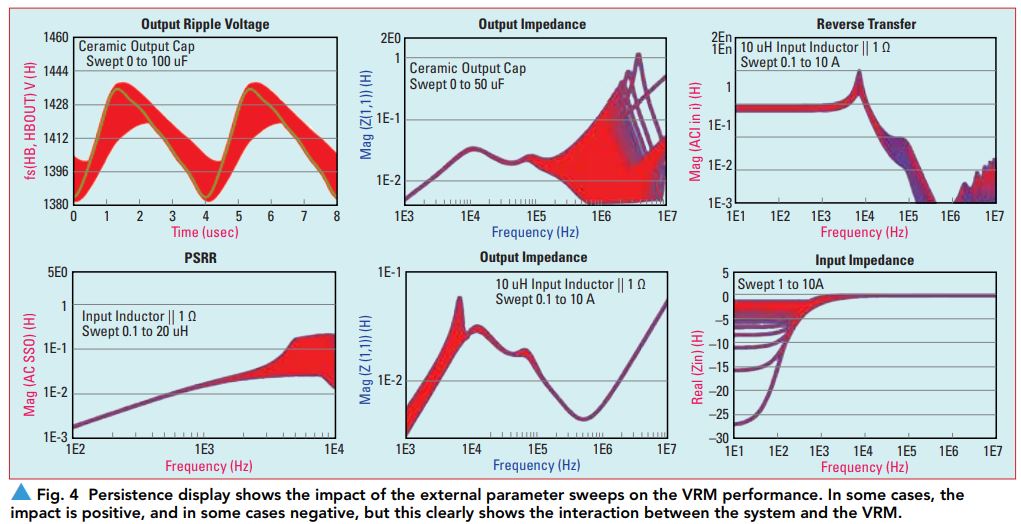
Persistence displays capture all the simulated waveforms, shown in Figure 4. The additional ceramic capacitance reduces the switching output ripple voltage. The reverse transfer, reverse transfer Q and PSRR are all negatively impacted, showing peaks due to the input inductance. These impacts are most notable with the load current at its maximum of 10 A and less notable at lower operating current, due to the relationship to the current dependent negative resistance.
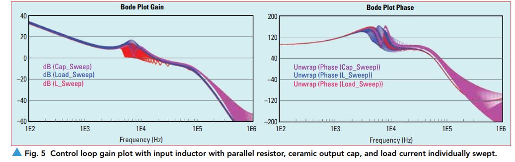
A single persistence display shows the control loop phase gain plot with the load current, the added ceramic output capacitor, and the input inductor with parallel resistor individually swept in a single display, shown in Figure 5.
 These simulations illustrate the significant interaction between the system and the VRM. It is important to consider all of the noise paths from the VRM and not just a small signal simplified resistor and inductor VRM representation.
Most notable in these simulations, the addition of the input filter inductor is seen in the output impedance and in the reverse transfer. The output impedance is negatively impacted by the input filter, affecting the transient induced voltages and target impedance performance. The input filter also introduces a high Q reverse transfer peak, potentially even oscillations. These result in load current dynamic currents being amplified at the VRM input where they distribute throughout the system. The ceramic output capacitors are shown to have potentially negative impact, both due to the low ESR and also due to resonating with the output inductance from the converter output capacitor ESL and pin inductance.
Article was published in the SIJ July 2019 Print Issue, Design Tips: Page 46.
References
1. www.spi2017.org/slides/SPI2017_Measurement_Based_VRM_Modeling_Slides_v0p5.pdf
2. S. Sandler, “Measurement Based VRM Modeling,” Picotest, 2017, https://www.picotest.com/downloads/Measurement-Base-VRM-Model-Tutorial-Final-2017.pdf