

We usually associate problems with the power distribution network (PDN) as from excess VRM noise, or from transient current draw from the core or I/O drivers. But that’s not the only source of PDN noise. Some failures can arise from the dull, boring, mundane problems at DC.
A recent survey conducted by Altium among its users identified ten common failures from PDN problems. Figure 1 shows the various problems and how often they were presented by survey participants. The most commonly reported problem, by 42% of the participants, is inaccurate values returned by analog front ends. This is often due to IR drops in power or ground paths. A few of the other problems reported were from thermal failures due to high current hot spots.
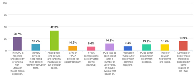
Figure 1. The top ten PDN problems reported by Altium users in a recent survey.
Some of these problems could have been identified by a DC analysis of the current flows in the power and ground paths. That’s exactly what the PDN Analyzer powered by CST does, available as an extension in the latest release of Altium Designer. John Magyar, Sr. Application Engineer with Altium, presented an overview of this tool at the recent Altium Live Event in San Diego on Oct 3, 2018.
“We see just as many customers worrying about DC current density and voltage drops in high current applications as low current applications,” Magyar said. “In high current applications, it’s a question of adding as much copper as you can afford and checking to see if it is enough. In some low current applications, like wearables and aerospace, it’s a question of removing as much copper as you can and making sure there is enough left.”
There are generally two issues with DC current in the PDN: the voltage drop from overall IR drops and the current density which translated into thermal hot spots. Figure 2 is an example of a map of the voltage drop on a power trace from a VRM to the input power pins of a consumer chip with its load.
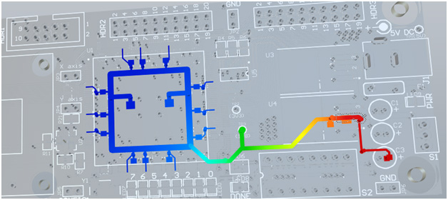
Figure 2. Mapping the voltage drop on the power path from the VRM on the right, to the IC power pins on the left. Red is higher voltage, blue is lower voltage. The entire color scale spans 30 mV out of a 1.8 V rail.
In this example, the power path, delivering 1.8 V, shows a voltage drop of 30 mV. This IR drop is 1.5% of the rail voltage, based on assumptions for the worst-case current usage by the IC. In this analysis, all the IC pins are connected together inside the chip, but the relative current flow into each pin is governed by the voltage distribution to each pin.
The second problem relates to the current density through each element of the PDN. This analysis can identify local hot spots which might translate into thermal hotspots. Figure 3 shows an example of a 3-D view of the current density in the ground distribution of a board.

Figure 3. Close up of a 3D view of two metal layers in a board. The red color denotes higher current density (40 A/mm2 ), while the blue is lowest current density.
Feeding into the via from the top layer to the bottom layer is a high current density region. This is partly due to the thermal relief connections to the via and the large plane cut-outs in proximity to this via.
The problem with high current density is that this translates into high power dissipation regions. It’s sometimes difficult to get a handle on the maximum current density acceptable in applications since it is all about the thermal environment the traces sees.
As a rough comparison, the IPC2221 recommendation for the maximum acceptable current in a 6 mil wide, 1 oz copper trace suggests 0.6 A as the maximum current. This corresponds to a current density of about 100 A/mm2. For this 1.8 V rail, the current density is within 50% of the range allowed in traces.
“The key feature of a tool like this is that it gives designers a visualization of the DC current flows,” Magyar said. While some problems may be obvious at a glance, the current flows in a large board with many cut outs and circuitous routes are hard to imagine. Evaluating the DC current distribution problems early in the layout phase might suggest regions that deserve a second look to reduce current density, IR drops, and risk.