RSS
RSS
The memory wall, once a niche topic for computer architects arguing over cache hierarchies, now shapes how AI data centers are physically built. As large language models move from training into round-the-clock inference, the industry is now pushing against the limits of physics. The problem is how to move enough bytes between memory and logic, and between accelerators, within the loss, noise, power, and thermal budgets of copper, optics, and power delivery networks.
The term was coined in 1995, when Wulf and McKee observed that processor speed was improving faster than DRAM speed and that, both trends being exponential, the gap would eventually dominate system performance.1 Three decades later, Gholami et al. quantified the same divergence for AI hardware: over the last 20 years, peak server compute scaled at about 3.0× every two years, DRAM bandwidth at 1.6× and interconnect bandwidth at only 1.4×.2 Compounded, this is roughly 60,000× more compute fed by 100× more memory bandwidth and 30× more interconnect bandwidth (see Figure 1). The industry answers on two fronts, both of which are interconnect problems: bring more bandwidth next to the die with high-bandwidth memory (HBM) and let many accelerators share their memory as one pool through scale-up networks.
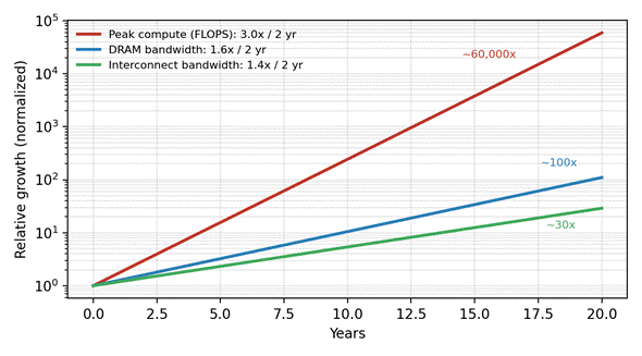
Figure 1 Normalized growth of peak compute, DRAM bandwidth and interconnect bandwidth, based on the scaling rates reported by Gholami et al.2
INFERENCE: MEMORY-BOUND BEFORE COMPUTE-BOUND
Serving a 70B-parameter model in FP16 requires 140 GB of weights, more than the 80 GB of a single H100-class GPU. Split across two GPUs with tensor parallelism, each GPU holds 70 GB of weights, all of which must be read from its HBM for every decoded token, together with its share of the growing key-value (KV) cache, while the two GPUs exchange partial results over the scale-up interconnect, for example NVLink, twice per layer. At 3.35 TB/s per GPU, the weight read alone takes about 21 ms per token. By contrast, the computation itself is small: generating one token takes about 1.4×10¹¹ FLOPs, or half of that on each GPU. Even at a conservative 500 TFLOP/s, each GPU completes its share in about 0.14 ms, some 150 times less than the 21 ms spent reading the weights. The compute units are idle more than 99 percent of the time.
The newest accelerators widen this gap. A Rubin-class GPU is previewed at roughly 16.5 PFLOP/s in dense FP8 with 22 TB/s of HBM4 bandwidth, or about 750 FLOPs per byte, whereas single-stream FP8 decode needs about 2 FLOPs per weight byte. Balance is reached only by batching hundreds of requests, which is what the latency requirements of interactive inference constrain. Context length adds a capacity wall to the bandwidth wall: with grouped-query attention, a 70B-class model stores about 320 KB of KV cache per token, or about 40 GB for a single 128K-token sequence.
HBM4: THOUSANDS OF LINES AT GIGABITS PER SECOND
JEDEC JESD270-4 (HBM4) doubles the interface width to 2,048 bits per stack at up to 8 Gb/s per pin, for 2 TB/s per stack.3 Previewed accelerators already exceed this baseline. Assuming 288 GB of HBM4 implemented as eight 36 GB stacks delivering 22 TB/s in aggregate, each pin operates at about 10.7 Gb/s, across more than 16,000 single-ended data lines routed in interposers a few millimetres long.
The cost for such density is a stack of coupled SI and PI constraints, alongside thermal challenges such as crosstalk across thousands of parallel, lightly terminated lines, simultaneous switching noise on power rails, and the thermal gradient of 12- or 16-high DRAM die stacks placed next to a GPU die dissipating close to 2 kW. Memory power is no longer negligible either. Assuming a total memory access energy of 2 to 4 pJ/bit, covering DRAM core and I/O, sustaining 22 TB/s costs between 350 and 700 W within the package power budget, which makes HBM a major load in its own right on the package power delivery network (PDN).
SCALE-UP: MEMORY SEMANTICS OVER SERDES
Scale-up networks allow an accelerator to load from and store to the HBM of another accelerator with near-local semantics. They differ from scale-out fabrics in three ways. They are single-hop and Layer 2 only, with no IP routing. Error recovery and flow control are handled primarily hop by hop at the link layer, rather than relying mainly on an end-to-end transport as in scale-out: NVLink and UALink implement link-level replay and credit-based flow control natively, while Ethernet scale-up (ESUN, SUE / SUE-T) borrows the link-level retry (LLR) and credit-based flow control (CBFC) mechanisms defined by the Ultra Ethernet Consortium. And their bandwidth per accelerator is an order of magnitude higher: NVLink 6 is quoted at 3.6 TB/s per GPU, or 1.8 TB/s in each direction, compared with 100 to 200 GB/s per direction of scale-out bandwidth per GPU on 800G to 1.6T network interfaces.
Several approaches compete for this domain, as summarized in Table 1. Their protocols diverge, and so, to a lesser extent, do their physical layers. NVLink, UALink, and Ethernet scale-up rely on 200G-class SerDes of the same generation as IEEE 802.3dj (UALink and Ethernet scale-up reuse the 802.3dj PHY directly; NVLink uses NVIDIA’s own), with NVLink 6 offering a per-GPU bandwidth of 3.6 TB/s. PCIe-based scale-up instead runs on the PCIe PHY at 64 GT/s PAM4 (PCIe 6.0), moving to 128 GT/s with PCIe 7.0, and trades lane rate for an ecosystem that every CPU, NIC, and accelerator already supports.4-6
| NVLink 5/6 | UALink | Ethernet scale-up (ESUN / SUE) | PCIe-based |
Governance | NVIDIA proprietary; licensable via NVLink Fusion | UALink Consortium (1.0 Apr. 2025; 2.0 Apr. 2026) | OCP ESUN (1.0 Mar. 2026); Broadcom SUE | PCI-SIG; merchant switches |
Lane rate | 200G (NVLink 5); NVLink 6 lane rate not disclosed (3.6 TB/s per GPU) | 200G | 100G/200G Ethernet PHY (802.3ck/dj) | 64 GT/s (PCIe 6.0); 128 GT/s (PCIe 7.0) |
Domain size | 72 GPUs (NVL72); 576 GPU dies planned (NVL576) | Up to 1,024 accelerators | Set by switch radix, single tier (e.g., 64 × 1.6T ports at 102.4 Tb/s) | Up to ~80 per switch; 64–144 chips across a multi-switch fabric (AWS Trainium3, NeuronLink over PCIe Gen6 PHY) |
Link reliability | Link-level replay + credits | Link-level replay + credits | LLR + CBFC (UEC) | ACK/NAK replay + credits; FLIT mode + FEC |
Table 1 Main scale-up interconnect approaches, based on public announcements as of October 2026. In-house fabrics such as AMD Infinity Fabric and Google ICI are not shown.
The UALink 1.0 stack illustrates how tightly protocol and PHY are now co-designed. Transaction-layer flits are packed into 640-byte data-link flits, each mapped one-to-one onto an IEEE 802.3dj RS(544,514) forward error correction (FEC) codeword of 680 bytes on the wire. One uncorrectable codeword costs exactly one flit, which the data-link layer replays locally. Link reliability is therefore set by the statistical distribution of codeword errors, not by the raw bit error ratio (BER). What this means in practice depends on how the errors are distributed. An isolated uncorrectable codeword is a latency event, but correlated bursts across consecutive codewords reduce throughput. A pre-FEC BER limit alone is no longer a sufficient specification.
THE 224G COPPER BACKPLANE AND THE ROAD TO 448G
Today, scale-up domains are copper. In an NVL72 rack, compute and switch trays blind-mate into cable cartridges carrying about 5,000 twinax cables, more than 3 km of copper. Driving the same links optically would have cost an estimated 20 kW per rack in transceivers and retimers.7 Copper reach is shrinking quickly, however: passive cables span only about 1 m at 224 Gb/s per lane and less than 1 m at 400 Gb/s per lane, confining copper to trays, backplanes and the shortest in-rack links.14
At 200 Gb/s per lane (212.5 Gb/s PAM4, 106.25 GBd), the Nyquist frequency is 53.125 GHz. IEEE 802.3dj allocates a 40 dB die-to-die insertion-loss budget to 200GBASE-KR1, split in a symmetric link into about 11.5 dB per host and 17 dB for the cable assembly.8 Within such a budget, every connector transition, via stub and package escape matters: a residual via stub resonance or a 1 dB connector mismatch can consume the entire link margin.
The step to 448G is harder. The OIF CEI-448G framework, released in November 2025, keeps PAM4, PAM6, and PAM8 open as candidate modulations, while PAM8 seems to be now falling out of consideration.9 Figure 2 summarizes the trade-off. PAM4 at about 425 Gb/s pushes Nyquist beyond 100 GHz, where conductor and dielectric losses and package parasitics become extreme. PAM6 and PAM8 bring Nyquist back to about 85 and 71 GHz, but at an additional 4.4 and 7.4 dB of eye-amplitude penalty relative to PAM4. In each case, the burden shifts toward equalization, FEC, and DSP power.
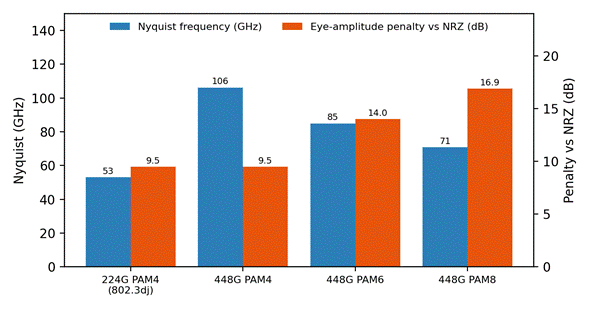
Figure 2 Nyquist frequency and ideal eye-amplitude penalty relative to NRZ, 20·log10(M−1), for 224G PAM4 and candidate 448G modulations, assuming a line rate of about 425 Gb/s and about 2.5 bits/symbol for PAM6.
The optical path for scale-up takes the opposite direction. The Optical Compute Interconnect (OCI) multi-source agreement, formed in March 2026 by AMD, Broadcom, Meta, Microsoft, NVIDIA, and OpenAI, specifies NRZ at 53.125 GBd over four wavelengths per direction, or about 200 Gb/s per direction per fiber, with the optics placed at the silicon rather than in a pluggable module.10 Rather than packing more bits per symbol into a lossy channel, it shortens the electrical channel to millimetres and multiplies wavelengths. The SI problem moves into the package, with die-to-optical-engine interfaces, laser and driver noise coupling and thermal crosstalk.
ADVANCED PACKAGING: THE PACKAGE BECOMES THE SYSTEM BOARD
Much of the battle against the memory wall is now fought in the package. With a monolithic die capped at one reticle field (about 858 mm²), AI accelerators and switches are assembled from multiple dies and HBM stacks on 2.5D interposers or embedded bridges; TSMC’s CoWoS-L reaches about 5.5 reticle fields with up to 12 HBM stacks in 2026.12 In 3D, hybrid bonding at 6–9 µm pitch replaces 25–55 µm microbumps, a 4× finer pitch giving 16× more connections per square millimetre.
Each step from PCB (75 – 100 µm line/space) to ABF substrate (8 – 15 µm), RDL (~2 µm) and silicon interposer (<1 µm) changes which physics dominates signal propagation, and every transition adds its own SI challenge. At interposer scale, a 1 µm × 1 µm copper trace has about 17 Ω/mm, so routes behave as distributed RC lines rather than transmission lines. This is why HBM and UCIe rely on thousands of short, wide, moderate-rate lanes, where crosstalk and simultaneous switching noise, not insertion loss, set the margin. In the substrate, the same package must route 200G SerDes as controlled-impedance transmission lines, through bump, via and ball transitions that each add reflections and consume part of the 40 dB budget, next to kiloampere power planes in 16 to 20+ ABF layers. Silicon-to-laminate CTE mismatch adds warpage, motivating glass cores. Thermally, 3D stacking forces heat from buried dies through the layers above.
Co-packaged optics (CPO) shortens the electrical channel to a few millimetres, with NVIDIA reporting up to 5× better power efficiency for its photonics switches.13 The price to pay is temperature-sensitive lasers next to kilowatt-class dies, and the loss of the pluggable optic as a test and service point. Socketed optical engines, such as those being standardized by the Open CPX MSA, aim to restore part of that serviceability.14
POWER INTEGRITY: MICROOHMS AT THE DIE, MEGAWATTS AT THE ROW
The PI challenge scales at both ends of the power chain. At the die, an accelerator approaching 2 kW on a core rail of about 0.75 V draws up to about 2,700 A, depending on how much of the package power flows through the core rail. With accelerator power projected to grow by about 500 W per year and exceed 4 kW by 2027, these currents could double.14 Assuming a 3 percent ripple budget and a 1,000 A load step, consistent with the synchronized compute and communication phases of collective operations, the PDN target impedance is about 22 µΩ, to be held flat from DC to well beyond the voltage regulator loop bandwidth. This drives vertical power delivery beneath the package, embedded and on-package capacitance and backside power networks in leading-edge process nodes. It also strengthens the coupling between PI and SI: at these currents, supply noise directly converts into jitter on 106 GBd SerDes lanes and timing noise on 10 Gb/s HBM pins.
At the rack, NVL72-class systems operate at about 120 kW. NVIDIA's Kyber rack for NVL576 targets about 600 kW, and the company has proposed an 800 VDC distribution architecture for 1 MW racks from 2027, with 64:1 DC/DC converters stepping 800 V down to 12 V near the GPU.11 600 kW at 54 V means about 11,000 A of busbar current; at 800 V, it drops to 750 A, and the resistive loss of a given conductor falls by a factor of about 220. This means that fast-switching, wide-bandgap converters with high dV/dt now operate centimeters from 200G SerDes. EMC, PI, and SI have to be engineered together.
THE ROAD AHEAD: CO-DESIGN AND BUILT-IN OBSERVABILITY
For the SI and PI community, there are four main takeaways.
First, channels must be designed as systems. The 40 dB budget at 224G, and whatever emerges at 448G, is shared among package, board, connector, and cable suppliers, which makes shared measured models and compliance metrics such as channel operating margin (COM) and effective return loss (ERL) more valuable than any single component specification.
Second, error statistics are replacing error rates. With flit-to-codeword mapping and link-level replay, what matters is the distribution of uncorrectable codewords and burst lengths under realistic traffic and realistic PDN noise, measured at the protocol layer as well as at the PHY.
Third, SI and PI can no longer be signed off separately, since supply-induced jitter becomes a first-order term in the link budget.
Fourth, physical access is vanishing. Scale-up links have no front-panel ports, run through blind-mate cartridges today and will terminate in optics on the package tomorrow. NVIDIA’s roadmap, for example, brings co-packaged optics to NVLink 8 for 1,152-GPU scale-up domains in 2028.14 Links will have to report on their own health through on-die eye monitors, FEC histograms, and standardized telemetry. In parallel, test and measurement (T&M) manufacturers will have to find ways back into the channel, notably through dedicated, customized interposers inserted at cable cartridges, connectors or package sockets, which tap or emulate the link while consuming as little as possible of its loss budget, and whose own effect is de-embedded from the measurement. Interposers are already the standard access method for PCIe and CXL protocol analysis inside servers; scale-up fabrics will demand the same approach at 200G per lane and beyond.
As inference becomes the dominant AI workload and scale-up domains grow from 72 toward a thousand or more accelerators, the memory wall will increasingly be addressed in the copper, the optics and the power delivery surrounding the processor. Signal and power integrity engineering will be a significant contributor to AI system performance and a key enabler of AI at scale.
Acknowledgments
The author thanks Wally Wardak at VIAVI Solutions for his review and inputs.
References
- W. A. Wulf and S. A. McKee, “Hitting the Memory Wall: Implications of the Obvious,” ACM SIGARCH Computer Architecture News, Vol. 23, No. 1, March 1995, pp. 20–24.
- A. Gholami, Z. Yao, S. Kim, C. Hooper, M. W. Mahoney and K. Keutzer, “AI and Memory Wall,” IEEE Micro, 2024 (arXiv:2403.14123).
- JEDEC, “High Bandwidth Memory (HBM4) DRAM,” JESD270-4, April 2025.
- UALink Consortium, “UALink 200G 1.0 Specification,” April 2025, and “UALink 2.0 Specification,” April 2026.
- Open Compute Project, “OCP ESUN – Network Operator Requirements – Base Specification 1.0,” March 2026.
- NVIDIA, “NVLink and NVLink Switch,” Technical Overview, 2025–2026.
- D. Patel et al., “Nvidia’s Optical Boogeyman – NVL72, Infiniband Scale Out, 800G & 1.6T Ramp,” SemiAnalysis, March 2024.
- C. DiMinico, Contribution diminico_3dj_01b_2307 on 200 Gb/s per lane electrical channel loss allocations, IEEE P802.3dj Task Force, July 2023.
- OIF, “Next Generation CEI-448G Framework Document,” November 2025.
- Optical Compute Interconnect MSA, “AMD, Broadcom, Meta, Microsoft, NVIDIA and OpenAI Form Optical Compute Interconnect MSA,” Press Release, March 12, 2026.
- NVIDIA, “NVIDIA 800 V HVDC Architecture Will Power the Next Generation of AI Factories,” NVIDIA Technical Blog, 2025.
- TSMC, CoWoS-L (3DFabric) packaging roadmap, as reported by Tom’s Hardware, 2026.
- NVIDIA, Rubin platform and Spectrum-X Ethernet Photonics announcement, CES, January 2026.
- AvidThink, “Data Center Networking in 2026: Scaling to New Heights: Up, Out, and Across,” Research Brief, 2026.