
The usual way of signaling through PCB interconnects is with two-level pulses, encoding of 1s and 0s or bits. It is called NRZ (not return to zero) or PAM-2 line code type. However, increased data rates with NRZ code has led to some obstacles. For a 28 Gbps NRZ signal, the bit time is about 35.7 ps with the main spectral lobe below 28 GHz. For a 56 Gbps NRZ signal, the bit time is about 17. 86 ps with the main spectral lobe below 56 GHz. One can see the problem already: getting PCB interconnect analysis and measurements up to 56 GHz and beyond is very challenging, to say the least. In addition, the expected attenuation (dielectric, conductor and roughness losses) will be also an obstacle for 56 GHz NRZ.
To reduce the bandwidth of the signal, pulse amplitude modulation with 4 levels, or PAM-4, is being used more on production boards. Instead of as single bits, symbols 00, 01, 10, and 11 are coded by 4 levels of the pulse, and the symbol time is two times larger than the bit time for NRZ signal with the same data rate. That is about 35.7 ps for 56 Gbps PAM-4 - same as for 28 Gbps NRZ! If we know how to design interconnects that correlate with the measurements for 28 Gbps NRZ, is it going to be "free lunch" to move to 56 Gbps NRZ? Not so easily, as I learned from the Alex Manukovsky's tutorial "A step by step guide for channel modeling & simulation that correlate to lab measurement for 25 Gb NRZ & 56 Gb PAM4 applications" and the panel discussion "The Case of the Closing Eyes: Is PAM the Answer? Is NRZ dead?" at the recent DesignCon2018.
So, to see the problem, I decided to do a numerical experiment and compare the predictability of the interconnects for NRZ and PAM-4 signals for the test board EvR-1 featured in our DesignCon2018 paper M. Marin, Y. Shlepnev "40 GHz PCB Interconnect Validation: Expectations vs. Reality" (The paper and complete report are available here.)
We used the "sink or swim" formula for predictable interconnect design that is is based on these components: interconnect geometry adjustments + identified material models + validated software -> predictable interconnects. With all three components in place, we were able to reliably predict behavior of most of the interconnect structures on an EvR-1 board without additional tuning or calibration for a 28-30 Gbps NRZ signal. For instance, here is a simple differential link with two segments of 1.1 inch microstrip line, two pairs of back-drilled vias, 1.5 inch of strip line and four press-fit connector and launches, to do the measurements:
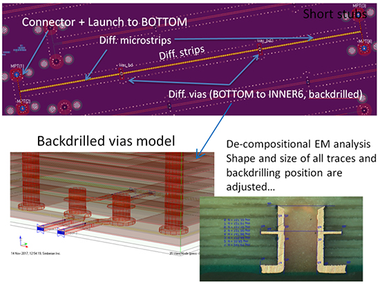
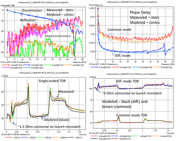
The vias, trace size, and shapes are adjusted to match the actually manufactured structures (remember, the boards are not manufactured as designed). The dielectric and conductor roughness models are identified with S-parameters measured for 2 differential microstrip and 2 differential strip segments using GMS-parameters technique with proper loss dielectric and conductor loss separation (see details in the paper). The analysis to measurement correlation in the frequency domain was acceptable up to 30 GHz, and TDR showed variations consistent with the low-cost PCB interconnects:
This correlation was actually sufficient to reliably predict the eye diagram for 28 Gbps NRZ signal as follows (15 ps rise and fall time, PRBS-32):
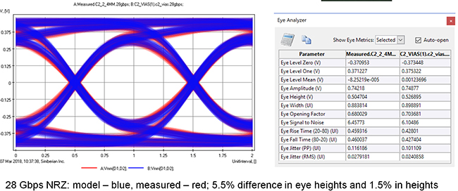
5.5% difference in the eye heights and just 1.5% in eye widths is not actually bad, considering the low-cost manufacturing very similar to the production boards. Now, let's try to predict 56 Gbps PAM-4 with exactly the same 15 ps rise and fall time and PRBS-32:
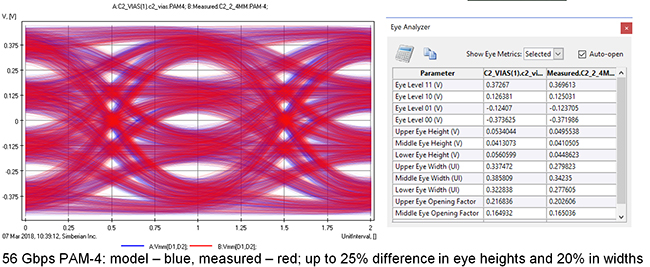
There is relatively small amplitude error. In the case of NRZ, there is now about 25% error! The eye width is not predicted accurately either. What is the problem? Obviously, we have smaller eye openings for three eyes and, naturally, the relative error increased. Let's look at the spectra of the signals used to generate the eye diagrams above (computed with DFFT for the finite sequence of bits and symbols):
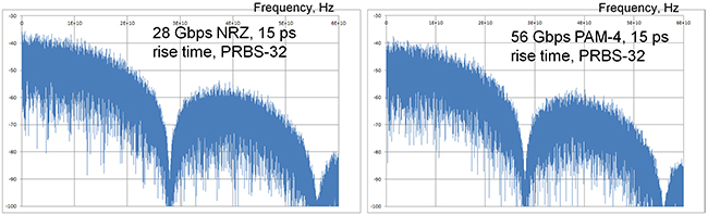
The NRZ signal in this case has about two times more power, comparing to the PAM-4 signal with the double data rate and the same rise/fall time and the same amplitude. The ratio of the power in the second lobe to the first one is about the same for both signal types. The bit time of the 28 Gbps NRZ signal is equal to the symbol time of the 56 Gbps PAM-4 signal. The accuracy of the analysis for both signals depends on the accuracy of the model above 28 GHz, which is where the second lobe of the spectrum is located. The model in this case does not correlate with the measurements above about 30 GHz due to the loss of the localization properties by the vias. This inaccuracy did not prevent an acceptable correlation for 28 Gbps NRZ signal. However, it degraded the accuracy of the model with 56 Gbps PAM-4. It looks like the signal energy above 28 GHz is more important to account for in this case, to have the analysis that correlate with the measurements. The absence of the correlation would probably not prevent the link operation in this case – the slight eye degradation will be handled by the adaptive Rx/Tx. This may be different for links at the border of the Tx/Rx compliance margins.
The bottom line is that the modeling of PAM-4 links with double data rates is more challenging compared to NRZ. The correlation bandwidth of the models should be extended forPAM-4. It means that the design process must include manufacturing adjustments and material model identification, and, most importantly, the interconnect analysis software should be validated up to 40-50 GHz for 56 Gbps PAM-4 links. It may sound ridiculous, but most of the interconnect analysis tools are not validated and, moreover, cannot be validated. The key in the validation is to make the minimal number of initial steps (geometry adjustments and material model identification) and apply the tool to typical interconnect structures without further adjustments. We introduced this with the CMP-28 board with Wild River Technology about 5 years ago and demonstrated on EvR-1 board with Marko Marin from Infinera at DesignCon2018. This is all about building the process and validating the tools. Advice: Do not trust the tool vendors just because of you paid a lot for it, or it is “3D electromagnetic,” or the marketing says that the tool is accurate and even “intelligent” and validated and show a couple of cases. VALIDATE EVERYTHING!