
Crosstalk in PCB and packaging interconnects is arguably one of the most complicated phenomena that may cause signal degradation. It is caused by unwanted coupling between signal links and power distribution systems. The effect is deterministic, but very difficult to predict in many cases—too many variables and uncertainties. Crosstalk effects can be treated statistically as a deterministic jitter with a bounded distribution, but the distribution is usually not known and just guessed. A direct analysis of a worst-case crosstalk scenario may lead to a system overdesign. Neglecting it in design may cause a system failure that is difficult to find and fix later in a design process. On top of that, distortions caused by crosstalk cannot be corrected by signal conditioning techniques at a receiver side. Thus, it is very important to understand the sources of crosstalk, how to quantify it and how to mitigate it efficiently. The first part of the paper includes an overview of crosstalk sources and terminology—just a slice through the complicated phenomenon. The second part will describe and compare different ways to quantify, compute, and measure crosstalk. This paper continues the “How Interconnects Work” series.1,2,3,4
Crosstalk in the Balance of Power
The best way to describe “what happens to a signal on the way to the receiver” is to use the balance of power that can be written for a passive interconnect as follows4:
P_out = P_in - P_absorbed - P_reflected - P_leaked + P_coupled
This is applicable to both the time domain and the frequency domain over the bandwidth of a signal as defined in.1 P_in is the power delivered by a transmitter to the interconnect (useful signal) and P_out is the power delivered to a receiver (degraded useful signal and noise). All other terms in the balance of power equation describe the signal distortion. The absorption and reflection terms (P_absorbed and P_reflected) were discussed in the previous papers of the “How Interconnects Work” series.2,3,4 This paper is about P_leaked and P_coupled or the crosstalk parameters.
P_leaked is a power leaked into other coupled interconnects, into the common mode and, possibly, into power distribution network (PDN is just another type of interconnects), and into free space (radiated)—that leak causes signal distortion and is a possible source of crosstalk, in addition to being source of EMC/EMI.
P_coupled is a power gained from the other coupled interconnects, common mode, PDN, and free space—this is the crosstalk.
The crosstalk in general is just unwanted noise from the coupled structures (P_coupled) caused by unwanted signal leaks (P_leaked) that degrade the useful signal and may reduce the data transmission rate, and may even cause complete link failure.
Crosstalk Types
Unwanted coupling in PCB and packaging interconnects can be separated into a local and a distant coupling:
1. Local coupling between closely spaced traces and viaholes:
- Coupling in closely routed signal traces – the most common source of crosstalk;
- Common to differential mode interference and crosstalk due to modal transformations in differential pairs (caused by bends, asymmetry in routing, fiber weave effect);
- Local couplings through slots and cutouts in reference planes;
- Local coupling between viaholes and between viaholes and traces due to proximity;
2. Distant coupling through parallel planes and split-planes (slots), and through surface dielectric layers and PCB enclosure (multipath propagation).
The local couplings can be accurately simulated in general and taken into account during pre- and post-layout signal integrity analysis. Simbeor SDK provides multiple kits for the pre-layout solution space exploration that takes into account crosstalk. Simbeor SI Compliance Analyzer provides unique capabilities for the fast and easy post-layout analysis of crosstalk, with the possibility of analysis and compliance verification automation.
Coupling in parallel traces can cause not only crosstalk and interference (unwanted noise), but also additional losses due to signal energy leaks to adjacent links (suck outs)—this is P_leaked term in the balance of power. The leak losses may be significant in traces routed on the surface of PCB (microstrips), though they are usually negligible for traces routed between parallel planes (striplines).
The distant coupling may cause a system-level interference and requires complete PCB or package analysis. The distant system-level coupling is very difficult to model and predict with sufficient accuracy. However, it can be either avoided (no rouging over split planes) or easily reduced by enforcing the localization for each structure that may potentially be coupled to parallel planes (transmission planes), surface dielectric layers, or to enclosure. Such coupling occurs at locations of changes in reference conductors. Un-localized viaholes are the major source of leaks and crosstalk, and can be easily avoided with the use of more stitching vias closer to signal vias, for instance. The system-level interference must be avoided by use of only the structures that are predictably localized up to the target frequency (conditional localization). Simbeor SI Compliance Analyzer has unique capability to verify the localization and find sources of potential system-level coupling during the reference integrity analysis.
Crosstalk Origin
PCB and packaging interconnects, such as striplines, microstrip lines, and coplanar waveguides are open waveguiding structures. It means that the signal energy propagates along the PCB and packaging traces mostly in dielectrics around the signal conductors. It can be illustrated with the peak power flow density (vector product of electric and magnetic field) for a typical PCB stripline interconnect, as shown in Figure 1. This is the peak power flow density (PDF) of a signal with 0.5 V magnitude, normalized to maximal value and expressed in dB as 10*log|P|.
 Figure 1. Power flow density in stripline 1.2 mil thick, 7 mil wide, DK=3.76, LT = 0.006 @ 1 GHz, planes 0.77 mil thick, 17.2 mil apart. Color scale is used to plot peak power flow density in W/m^2, computed with Simbeor THz.
As you can see, there is no exact localization of the signal energy. The power flow density or signal energy concentrates near the strip edges and between the strip and planes. The red and yellow area is where the most of the signal energy propagates. But it is also non-negligible in the green area of 2-3 strip widths, in this case. Everything that gets into zone with green PFD (-25 to -30 dB level, 2-3 width of strip on both sides) becomes coupled, and that coupling may cause interference or crosstalk and signal leaks. In addition, the coupling changes the strip impedance. Figure 1 depicts the dominant strip line mode that has equipotential reference planes.
The signal energy spreading around a signal conductor is even worse in traces routed on a surface of PCB (microstrips) as we can see from the Figure 2.
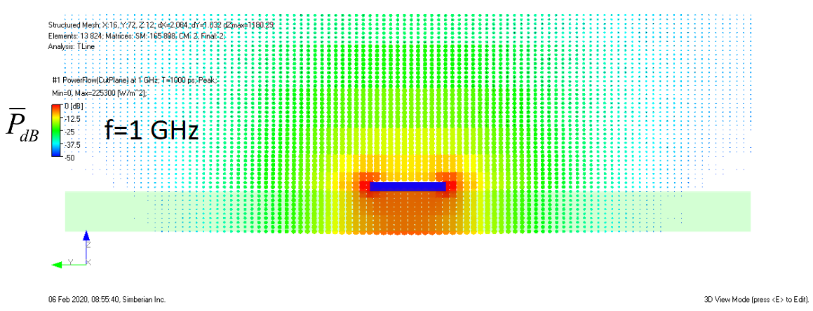 Figure 2. Peak values of power flow density at 1 GHz in microstrip line with 8.256 mil wide trace on 4.5 mil FR4 substrate.
As we can see, the area of potential coupling is larger in the air as well as in the substrate; the trace can be effectively coupled to nearby traces as well as to any external objects that are in the area with green PFD (-25 to -30 dB).
Similar or even worse extension of the coupling area can be observed in unsymmetrical strip lines, as illustrated in Figure 3.
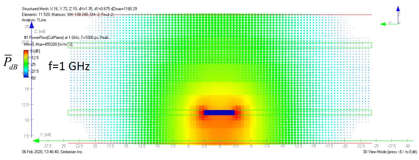 Figure 3. Peak values of power flow density at 1 GHz in unsymmetric strip line with 5.4 mil trace, distance from strip to top plane 9.77 mil, distance to bottom plane 4.5 mil, DK = 4.2 (~50 Ω).
 Figure 4. Peak values of power flow density at 1 GHz of differential mode in differential microstrip line with 7.446 mil traces on 4.5 mil on substrate DK=4.1 (~100 Ω).
 Figure 5. Peak values of power flow density at 1 GHz of differential mode in unsymmetrical stripline with 4.674 mil wide strips, distance from strip to the top plane 9.77 mil, to the bottom plane 4.5 mil, DK = 4.2 (~100 Ω).
Differential mode in loosely coupled differential traces has signal energy spread similarly to the single-ended case, as illustrated by the peak power flow density for a typical differential microstrip in Figure 4. Peak PFD for a differential mode in a differential stripline with unsymmetrical reference planes is shown in Figure 5. As we can see, the distant reference planes may substantially increase the area where strips can be coupled, even in the differential cases. The PFDs in Figure 4 and Figure 5 are for the differential modes with excitation +0.5/-0.5 V. The power of the differential mode flows around each trace in the same direction mostly along the traces.
If you still think in terms of currents, please quit. The currents at microwave frequencies are not “flowing” and not “returning” anywhere—they are just a part of the wave propagation process and conductor energy absorption. The power flow density is the best way to visualize the physics of a signal propagation. The surface currents in the reference conductors can be also used to evaluate possible coupling areas, but it is not so intuitive and obvious as with the PFD. In general, it is important to understand that a single trace is a two-conductor transmission line or waveguiding structure—the second conductor is always the reference plane (microstrip) or two planes (stripline). Differential traces are a three-conductor transmission line, and the currents in the reference conductor are also spreading beyond the traces similar to the single-ended cases. Reference conductors or planes in the signal energy propagation area are as important as the traces themselves. In a case of two reference planes, the equipotentiality of the planes along the signal propagation must be ensured with more stitching vias, and even via fences, to avoid coupling to the dominant mode of the parallel plane structures—such coupling may occur at discontinuities such as viaholes and dielectric inhomogeneities. Enforcement of the reference equipotentiality for coplanar transmission lines is even more complicated.
The bottom line is that the PCB and packaging interconnects are the open waveguiding structures with the signals propagating in space around the signal traces. Getting a signal with spectrum in microwave and millimeter-wave bandwidth from one component to another through an open waveguiding structure and without interaction with other signals is always a challenge. See more on different signal couplings cases in “How Interconnects Work™” demo-videos at either the Simberian website or @simbeor YouTube channel.
Useful Crosstalk Terminology
Before proceeding with crosstalk modeling and quantification, let’s define some common terms.
Stripline: model for traces routed on the internal layers of PCB/PKG with two reference planes and mostly homogeneous dielectric;
Microstrip line: model for traces routed on surface of PCB/PKG with one reference plane and inhomogeneous dielectric;
Coplanar line: model of traces with additional reference conductors in the same layer with the signal traces;
Aggressor: a transmitter (Tx) or a link with a signal that may cause interference in other links;
Victim: a receiver (Rx) or a link that may pick up unwanted interference caused by an aggressor link;
NEXT: near end crosstalk is interference observed at the link side that is closer to the aggressor link transmitter or signal source;
FEXT: far end crosstalk is interference observed at the link side opposite to the aggressor link transmitter or signal source;
There are many more terms for the crosstalk characterization. PSXT, MDXT, ICN, ICR, and some others will be introduced and explained in the upcoming section on crosstalk quantification.
Crosstalk in Parallel Traces
To illustrate interference of signals in parallel segments of microstrip line (surface trace), we will use two single-ended links routed at a distance equal to one trace width over 1 in. distance. The characteristic impedance of each single trace is close to 50 Ω . In the first case, a signal propagates in the top trace from port p1 to port p3, as illustrated Figure 6.
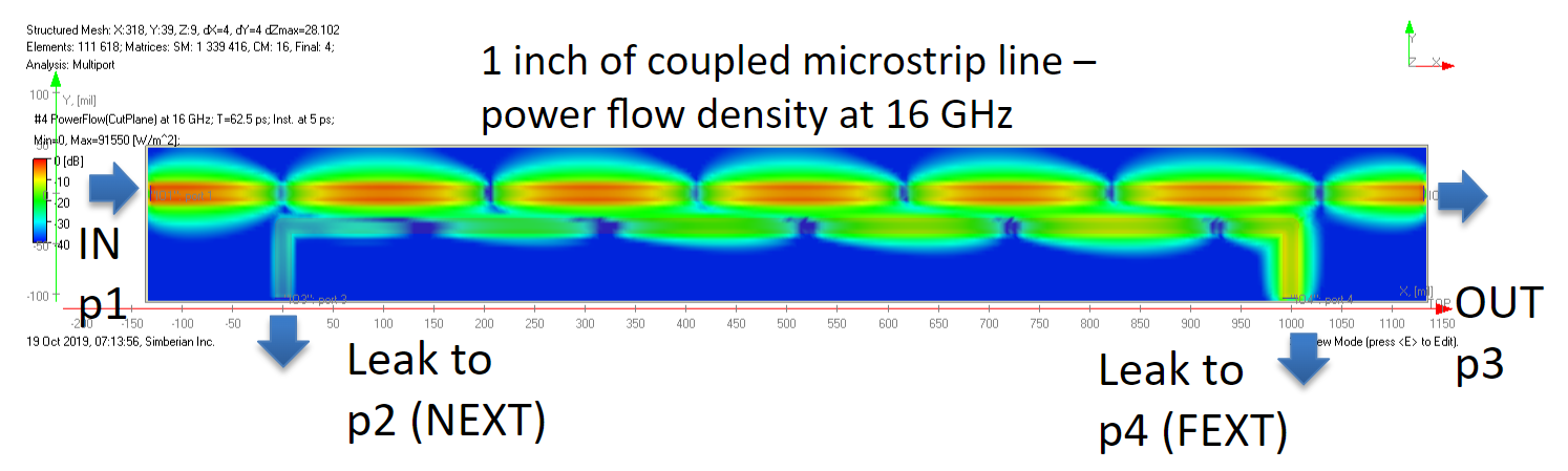 Figure 6. Instantaneous values of power flow density in dB with 16 GHz 0.5 V signal propagating from p1 to p2. 16 mil traces on 8 mil substrate with Dk=3.9 coupled over 1 in. with 16 mil separation.
As we can see, the bottom link with ports p2 and p4 is literally in the “signal space” of the top trace. As the consequence, the bottom trace is coupled and “sucks out” some signal energy. Some useful signal power leaks into port p2 near the signal source (NEXT) and into port p4 on the side opposite to the signal source (FEXT). The leak is the result of the wave energy redistribution over the length of the coupled segment. How much energy is leaked, and what are the consequences of that leak if there is a useful signal propagating in both links? The most fundamental and convenient way to describe this energy re-distribution phenomenon is with scattering parameters, or S-parameters.5 In case if you consider that as too long to read, there is shorter introduction into the subject.6 Even shorter one-paragraph introduction is provided in Appendix I. It is very important to get familiar with the S-parameters. In fact, practically all other interconnect quality metrics, including crosstalk quantification parameters, are simply derived from the S-parameters. Magnitudes of the S-parameters describing process of the energy re-distribution for the structure from Figure 6 are shown in Figure 7.
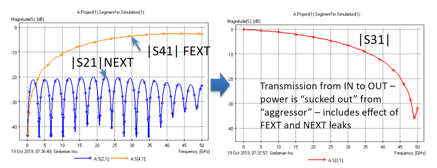 Figure 7. Magnitudes of coupling S-parameters (|S41|and |S21|on the left graph) and transmission parameter (|S31| on the right graph) for microstrip traces with 1 in. coupled segment from Figure 6.
Parameter S31 on the right graph of Figure 7 is the transmission of the useful signal from port p1 to port p3. Parameters S41 and S21 are the leaks and potential crosstalk parameters. As we can see, the transmission|S31| is decreasing with the frequency, but with a slope that is much steeper than expected due to the material absorption losses.2 The reflection, or return losses, are very small in this case. The reason for this is a leak into port p4 that is described by S-parameter S41 on the left graph in Figure 7. The leak into port p2 is much smaller in this case. With a useful signal at port p4, parameter S41 becomes Far End Crosstalk (FEXT). It is frequency-dependent, and the maxima and minima are defined by difference of propagation velocities of the even and odd modes in the coupled segment and by the segment length. There is no FEXT if this difference is zero or close to zero. FEXT can be observed in any lossy multi-conductor transmission line in general, but it becomes substantial only in cases of transmission lines with inhomogeneous dielectrics, such as microstrip lines, for instance. Striplines with dielectric layers with different properties also have observable and not-negligible FEXT. FEXT increases with the length of the coupled traces up to some level and then decreases, reaches minimum. Then minima and maxima repeat periodically with the frequency. In general, more energy from an aggressor link may leak into a victim link on links with longer coupling sections. The leak can interfere with the victim signal and degrade it. On the other hand, the leak also degrades the aggressor signal—it causes additional losses that can be comparable or even larger than the reflection and the material absorption losses. In fact, there might be conditions when almost all energy of the aggressor signal becomes FEXT. In the case above, almost complete suck out happens around 50 GHz. For the same traces coupled over longer 5-in. segment, the complete suck out would happen around 10 GHz, as illustrated in Figure 8—this is Nyquist frequency for 20 Gbps signal. Extensive simulations must be used to detect and avoid such conditions early in design process.
 Figure 8. Magnitudes of coupling S-parameters (|S41|and |S21|on the left graph) and transmission parameter (|S31| on the right graph) for microstrip traces with 5 in. coupled segment.
 Note that S-parameters of passive interconnects are reciprocal. This means that transmission from port i to port j is always equal to transmission in the opposite direction from port j to port i. This is not very intuitive property. Applying it to crosstalk, we can state that S41=S14, S21=S12; if the aggressor and the victim are switched, the crosstalk does not change. If the bottom link in Figure 6 has useful signal, then that link becomes aggressor for the top link, as illustrated in Figure 9. The top link is the aggressor for the bottom link, and the bottom link is the aggressor for the top link. The result is the superposition of signals in both links, and both links have FEXT.
 Figure 9. Crosstalk power flow density in coupled microstrip line segment from Figure 6 with two 16 GHz signals propagating in the same direction from p1 to p3 and from p2 to p4.
 Up to this point, we have investigated the coupling in the frequency domain or for the time-harmonic signals. However, digital signals are usually transmitted by pulses.1 Let’s take a look at the crosstalk in time domain. To do this, a pulse response can be computed from the S-parameters of the four-port structure, as illustrated in Figure 10.
 Figure 10. Frequency-domain FEXT and transmission parameters (left) with corresponding pulse responses (middle) and superposition of the pulse responses (right).
 Transmission from port p1 to port p3 is characterized by S-parameter S31 on the left graph, and corresponding pulse response shown in the middle graph in Figure 10. The bottom link is a potential aggressor in this case; it has leaked to port p3, as illustrated with S-parameter S32 in Figure 10. If the bottom link has similar pulse propagating from port p2 to p4, some part of the pulse energy is going to be leaked into port p3 of the top link. Corresponding pulse response for the crosstalk parameter is also shown in the middle graph in Figure 10. If both links have signals propagating in the same direction over the coupled segment, the signals at port p3 will be a superposition of the link pulse response and the crosstalk pulse response, as illustrated on the right graph in Figure 10. Because of the timing of the pulses at ports p1 and p2 are not synchronized, the crosstalk position is arbitrary with respect to the link pulse. That what makes the crosstalk difficult to quantify. We can find the worst-case relative timing, but it may never happen.
Let’s return to the near-end crosstalk. S-parameters S21, S12, S34, and S43 describe the near-end crosstalk (NEXT) in cases when the signals in the top and bottom links are propagating in the opposite directions, as illustrated in Figure 11. The NEXT is frequency-dependent and has nulls at frequencies where the coupled segment is about a multiple of half of wavelength, as illustrated in the left graph in Figure 12. The maxima in NEXT are approximately at frequencies with the wavelength equal to odd multiples of a quarter of a wavelength. The near end coupling depends on the length of the coupling section, though the frequency-domain pattern of the NEXT is considerably different from the FEXT.
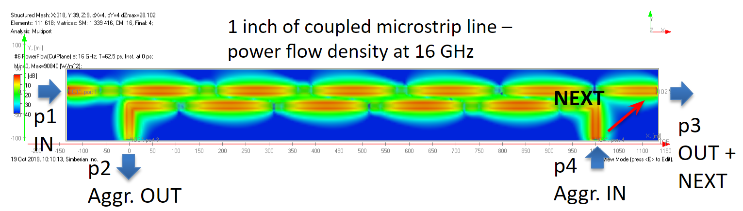 Figure 11. Crosstalk power flow density in coupled microstrip line segment from Figure 6 with two 16 GHz signals propagating in the opposite directions from p1 to p3 and from p4 to p2.
Figure 12. Frequency-domain NEXT and transmission parameters (left) with corresponding pulse responses (middle) and superposition of the pulse responses (right).
As we can see, the level of maxima of NEXT in this case is about -20 dB. That gives relatively small crosstalk pulse response (smaller than FEXT, in this case), as shown on the middle graph in Figure 12 together with the pulse transmitted from port p1 to port p3. It comes in two parts—the first appear at the victim port p3 almost immediately, and the second part appear with a delay. There might be no second part for a longer links with substantial attenuation. A superposition of the useful signal and crosstalk at the port p3 is shown on the right graph in Figure 12. As in the case of FEXT, timing of the NEXT with respect to the pulse of the useful signal is also arbitrary. Note that the signal in the victim link may be substantially attenuated at the received end; that means that much smaller values of NEXT can cause failure of the victim receiver. All coupled nets have NEXT. However, it is important how close to the victim receiver it appears.
Finally, here is how crosstalk in coupled transmission lines can be “explained”. A signal in multi-conductor interconnects propagates as a superposition of multi-conductor line modes—this is a model presentation, but it allows to understand what happens there and what to expect. For instance, a differential signal on the NEXT or FEXT aggressor side becomes a superposition of four waves in coupled two-conductor transmission line segment. Those are the even and odd modes propagation in both directions. The signal cannot remain on just one trace due to the coupling. The waves propagating toward the aggressor side are observed as the NEXT. The waves propagating forward from the aggressor are observed as the useful signal in the aggressor link and also as the FEXT at the victim port. If all modes have identical propagation velocity (which never happens in real lossy lines), there will be no FEXT. However, if the modes are not ideally terminated at both ends, the waves forming NEXT are reflected and may appear at the other end as the FEXT. Waves that compose FEXT can be also reflected and become NEXT. To understand different coupling outcomes, a lattice diagram with the transmission line modes superposition can be used, though the advanced modeling is the easier way to account for all those reflections.
Appendix I: S-Parameters at a Glance
All signal and power interconnects can be described as multiport or black-box structures with just ports sticking out as illustrated in Figure A1. Each port has two terminals—a signal terminal and a local reference terminal with currents and voltages defined, as also shown in Figure A1.
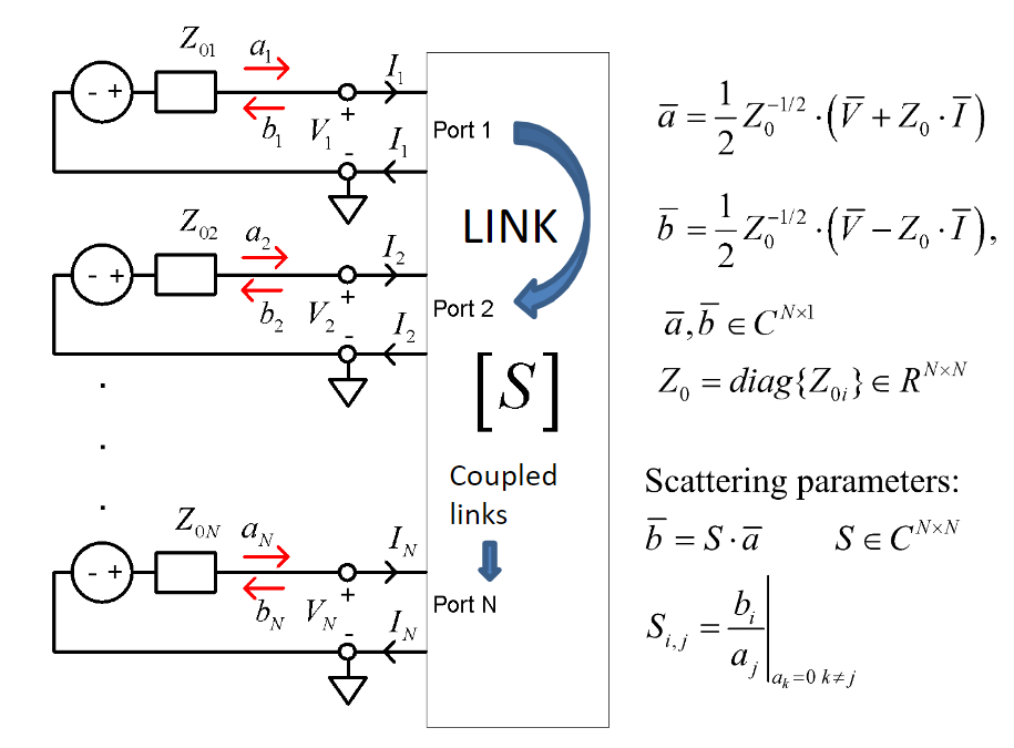 Figure A1. S-parameters definition.
With the currents and voltages, we can define Y-parameters (short-circuit parameters) and Z-parameters (open-circuit parameters). Though, instead of voltages and currents, S-parameters use “waves” defined at each port terminated with the normalization impedance Zo (that is usually just a resistance equal to 50 Ω ). The waves are variables that combine both current and voltage at each port in such way that the square of wave magnitude is the power of the wave. The waves may be real as in transmission line or, more often, are defined formally for modeling or measurement purpose.
Similar to the currents and voltages, waves have directions as shown in Figure A1. Incident waves (a=0.5*(I+Zo*V)/sqrt(Zo)) are directed into the multiport and reflected or outgoing waves (b=0.5*(I-Zo*V)/sqrt(Zo)) are directed from the multiport. S-parameters relate the incident and reflected/outgoing waves for each combination of ports terminated with the normalization impedance Zo. It is N by N matrix for the multiport shown above with the frequency-dependent elements. The matrix element Sij is the wave outgoing from port i (directed from multiport) with the unit incident wave at the port j only (no incident waves at all other ports). For passive interconnects, it means that the magnitudes of S-parameters are always bounded by 1—the power leaving the multiport should be always equal or smaller than power delivered to multiport.
In cases of transmission line ports with the normalization impedance equal (or about equal) to transmission line characteristic impedance, Sij can be interpreted as a voltage at port i created by incident voltage 1 V at port j. Magnitudes on the S-parameter graphs are usually plotted in dB versus frequency (SdB=20*log(|S|)). dB value can be converted back into S-parameter magnitude by simple conversion formula 10^(|SdB|/20). 0 dB corresponds to unit value—for transmission parameters, it means ideal transmission. For reflection parameters or return loss, 0 dB, or unit valuem means complete reflection or failure. -3dB corresponds to magnitude about 0.708 (or a half of power), -6dB to 0.5 (or a quarter of power), -20dB to 0.1, -40dB to 0.01, and so on. This is practically all you need to know about S-parameters, if you are not planning to write your own electromagnetic or signal integrity software.
REFERENCES
P. J. Pupalaikis, "S-parameters for Signal Integrity," Cambridge University Press, 2020.