
This article is a continuation of SI/PI problems and lessons that I have toiled through and would love to share with the community. I received positive feedback on my last article Mysterious Case of the Flapping Switch (https://www.signalintegrityjournal.com/blogs/11-engineering-nightmares/post/543-mysterious-case-of-the-flapping-switch), so I will continue to try to capture some interesting stories. Hopefully this will help others to quickly debug their lab nightmares.
We were nearing the final stages of designing a next generation set of blades that would upgrade already existing chassis in the field. We had more than doubled the backplane speed and had already performed significant SERDES pre-emphasis tuning and DVT. We were essentially getting ready to ramp up building the final set of line and fabric cards, so the schedule pressure was high.
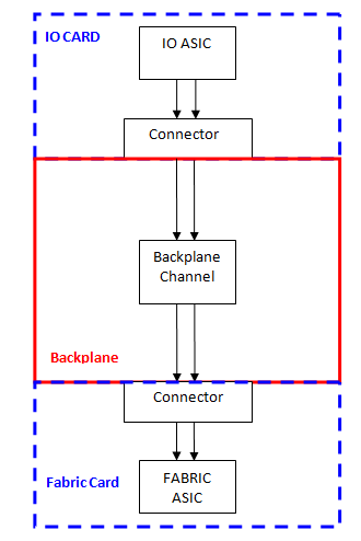
We started to run into CRC (cyclic redundancy check) errors in a few of our high-speed channels intermittently. The high-speed channels are pretty typical of what was appearing in the industry: about 30” long channels on FR4, high-speed connectors, line cards, going through a backplane then into a fabric card (see Figure 1). We were using a relatively new but very popular switch/fabric chip technology with the same vendor on both ends, so we didn’t need to worry about SERDES vendor mismatch issues. We also had done extensive simulation and testing on the channels and thought we would not have any issues.
These CRCs started to pop up as random failures in the lab and were confined to some of the longer channels (but not the longest). Some platforms would run error free, while others would exhibit errors more consistently.
Since the backplane design had already been shipping for years, changing backplane material, or connectors was not an option. What was particularly interesting was that these random errors happened at room temperature on select systems, but not all systems. We started collecting up a variety of test equipment to try and debug this issue. We had real-time and sampling high-speed scopes and a TDR. We spent the better part of a month working on this one issue from morning until late at night. This was holding up the possibility of shipping, and we had to hunker down and do whatever it took to get this problem resolved.
As I mentioned in my last article, once a problem is locally reproducible you can examine the usual suspects: software, hardware, layout, mechanical, power, clocks, and the channel. I started measuring the clocks on the local fabric card that exhibited the issue. Everything met specs, and, since we only saw an issue on one or two channels, we thought it was unlikely to be the clocks (they were common across all the channels).
Next we went on to analyze the power going into the fabric chip. There were multiple supplies with very tight DC and AC specifications. We measured all of the rails. We compared DC levels to specs, and AC levels and noise did not reveal anything suspicious. The SERDES power rails on chip drove four “quads,” so we thought it unlikely a local power issue, because more/all the SERDES in that quad would exhibit the issue. Next my colleague and I re-reviewed the layout. We observed some minor deficiencies but nothing that was a smoking gun. We repeated all of the measurements multiple times.
We examined the channel in time and frequency domain. We measured eyes of the good channel and the bad channel (see Figures 2 and 3). They looked very similar. Although the “bad channel” had a little more jitter and slightly worse eye, there was nothing there that we could put our finger on that would cause these types of CRC errors.
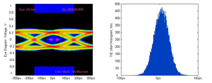
Figure 2: Eye and TIE of Bad channel

Figure 3: Eye and TIE of Good Channel
What was particularly frustrating is the errors seemed to come and go. Sometimes we would see a few every minute, other times we would go hours without any. We started exploring EMI/RFI issues. We wrapped local switching power supplies in copper foil, experimented with various types of shielding. When the VP of engineering came out and looked over my shoulder, he gasped in disbelief that we were going to have to implement some kind of elaborate shield. I explained to him we were just trying to root cause the problem and not necessarily come up with a fix.
I called a few industry experts who were colleagues that I have worked off and on with over the years. Everybody was stumped (although one offered to come help me for the standard consulting fee :-) ). We thought we were onto something when the errors would go away for a few hours, but then as quicky as they went, they came back. Finally, I decided to call one of the chip developers who was from Isreal and was an SI/RF expert as well as having intricate knowledge of the ASICs, I’ll call him “M” (Not to be confused with the James Bond fictional character head of MI6).
“M” was a very intelligent chap who had been working on these chips for a number years and knew the designs intimetly: the chips, SERDES, package, SI, PI, logic and SW (he is also the savior of another engineering nightmare). Usually system design engineers (ASIC customers) would never have access to the actual chip designers, but we were going to be very good customers and they were small enough to give us that extra customer service. I had been chatting with him off and on for years on a variety of issues, including sharing simulations and measurements results. He also had previously reviewed the original designs.
Since M’s wife was studing for her PHD in the US, it worked that we could negotiate with him to come for a visit. After travel arrangements were set up, M sent me a long list of equipment to get prior to his visit: high-speed scope, VNA, spectrum analyzer, phase noise analyzer, DVM, solder irons, traffic generator, BER tester, … Some of the equipment we had, the rest we begged and borrowed. A few things we went without.
When M arrived on a Monday morning we hit the ground running. One of the first things he did was pulled off the oscillator and replaced it with an SI_LAB PLL based oscillator. This had no effect on the CRC errors, but it improved the jitter profile enormously, and, as I have learned, it is one way to elimimate possible clocking errors.
When debugging problems, you need to be a detective and eliminate possiblilities one by one. He did all of his own soldering because he didn’t trust any lab techs to keep leads short and mimize loop inductance and not screw up. He taught me a lot of tricks that I never even dreamed of. Back of the envelope (literally) he designed and implemented power splitters from descretes and then professionally soldered them down into the channel so we could feed one output into a scope and another back into the channel. Since we didn’t have a VNA, he actually cascaded two high speed scopes, one looking in time domain, one looking at frequency domain, I had never seen anything quite like it before.
M wrote his own software including a previously written GUI that allowed us to run various pattern sets and payloads on the ASIC to aid debug. He mentioned in his earlier years he used to climb anntenas with a spectrum analyzer on his back and debug RF issues. Needless to say we were impressed with his broad and deep set of skills. It took us a month to do what he did in a week. It got close to the end of the 4rd day and look at me and said; “This problem may not be solvable.” He wasn’t trying to be arrogant, but continued “If I can’t solve it, it can’t be solved...”
We fired up his GUI and entered 101010101for transmitting payload with headers removed. The idea was any noise coupled onto the transmitted signal would show up in the frequency domain, because setting a fixed transmitted pattern of alternating ones and zeroes would result in a strong carrier frequency, eliminating any ISI or deterministic jitter, which can be easily viewed with a spectrum analyzer.
We remeasured the channel and all of sudden we noticed something in the channel. It was spurs ~ -47db down, and I saw a twinkle in his eye. He said we have to find where that is coming from and started going after the source (IO) board which we had almost completely ignored. He then started looking at the SERDES 1V0 with our newly borrowed spectrum analyzer. We probed the 1V0 SERDES switching supply on the source board power supply and we observed spurs that are increasing in amplitude with frequency (harmonics of the switching frequency) one particullaly worrisome @ -25.56 dB spur at ~ 2.5 Mhz (see Figure 4).

Figure 4: 1V SERDES Switching Supply IO ASIC
He then explained that the CDR (clock data recovery) circuit in the ASIC is particularly sensitive to noise in the region of 1MHz to 4MHz. Generally noise below 1MHz can be ignored because the PLL easily tracks these variations. The noise generated by the switching power supply (which supplies the ASICs) was significant in this region, and it was fed through right into the channel.
The idea of inserting a power splitter in the channel and driving alternating ones and zeroes down the channel was a great trick. We verified that the failing channel’s transmitted spectral content matched that of the 1.0V SERDES digital supply (see Figure 5). This signal would then be received by the downstream switch chip and cause its CDR to fail occasionally.
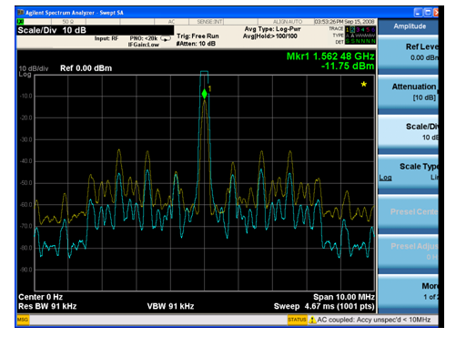
Figure 5: 1V Power Supply and Channel Spectrum overlay (different vertical scales)
So now that we had root caused what was causing the CRCs, it was a simple matter to try to improve or fix the switching power supply. Some of the older switching supplies are actually a lot less noisy than the newer ones. We pulled a switcher off of a previous generation board and soldered it onto this new generation board (Figure 6), again another small feat of magic.
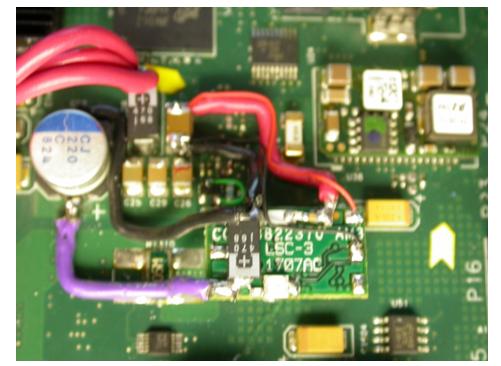
Figure 6: Old 1V Switcher, soldered down on new IO Card
Looking at the power spectrum before and after on the 1V0 SERDES voltage in the frequency domain is pretty dramatic (Figure 7-9):
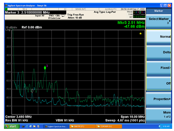
Figure 7: 1V0 SERDES Noise Before and After
The noise coupled into the channel at the driving ASIC also showed a huge improvement. So the answer was to have the right tools/equipment to debug the problem, people knowledgeable enough to know what to look for, and finally the ingenuity to create solutions by using what is at hand.
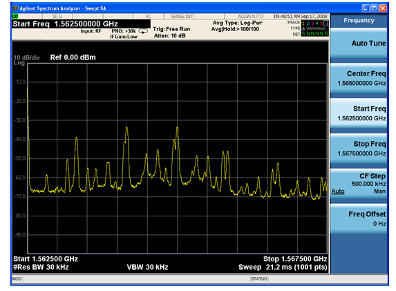
Figure 8: Original Channel Power Spectrum (running 101010 pattern) before 1V0 change
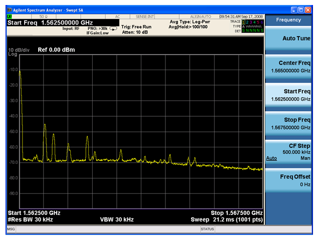
Figure 9: New Channel Power Spectrum (101010) after 1V0 change
The original switching power supply that we examined exhibited significant noise and is not suitable for providing power to parts that utilize a sensitive SERDES CDR. We ended up purchasing a modestly priced spectrum analyzer to assist with any future debug and DVT of power supply designs. In addition to cleaning up the power supply noise spectral issues, we cleaned up a variety of minor layout issues, and utilized a SI_LABS oscillator on both the IO and fabric blades to take advantage of its much better jitter characteristics. (It was also competitively priced). After solving the switching power supply noise issue, we were able to run a fully loaded chassis with all channels switching at full bandwidth over temperature without any CRCs.