
This paper was presented at EDI CON USA 2017
Multi-phase switching power supplies are utilized typically in applications requiring high currents where the current is supplied through multiple, independent phases of the supply. The design goal is for all of the phases to share current equally. These supplies are quite complicated from a control standpoint as there may be multiple control loops utilized to maintain proper current sharing. While a supply might operate properly most of the time, the measurement of the supply under various transient conditions is required to guarantee proper operation under all conditions.
The measurement of current sharing requires at least measurement of the inductor current and preferably a transient current generator including ideally a static direct current (DC) load. The measurement of inductor current is particularly problematic because it may require breaking the loop to provide for a current probe or modifications to the circuit to add various components.
In our presentation, we will demonstrate the use of a special probe tip utilized to convert a differential measurement of inductor voltage to a measurement of inductor current. We will demonstrate the connection and calibration considerations in the measurement of inductor current including the digital signal processing algorithms required to compensate for the components in the power supply and the probe tip. We will also demonstrate and explain current sharing measurements made in the time and frequency domain using a transient current generator.
Patent Disclosure
Portions of this document are the subject of patents applied for.
Disclaimer
This paper does not constitute as an endorsement by Oracle Corporation for any specific product, service, company, or solution.
Author(s) Biography
Peter J. Pupalaikis was born in Boston, Massachusetts in 1964 and received the B.S. degree in electrical engineering from Rutgers University, New Brunswick, New Jersey in 1988. He joined LeCroy Corporation (now Teledyne LeCroy), a manufacturer of high-performance measurement equipment located in Chestnut Ridge, New York in 1995 where he is currently Vice President, Technology Development, managing digital signal processing development and intellectual property. His interests include digital signal processing, applied mathematics, signal integrity and RF/microwave systems. Prior to LeCroy he served in the United States Army and has worked as an independent consultant in embedded systems design. Mr. Pupalaikis holds forty-three patents in the area of measurement instrument design and has contributed a chapter to one book on RF/microwave measurement techniques. In 2013 he became an IEEE fellow for contributions to high-speed waveform digitizing instruments. He is a member of Tau Beta Pi, Eta Kappa Nu and the IEEE signal processing, instrumentation, and microwave societies.
Istvan Novak is a Senior Principle Engineer at Oracle. Besides signal integrity design of high-speed serial and parallel buses, he is engaged in the design and characterization of power-distribution networks and packages for mid-range servers. He creates simulation models, and develops measurement techniques for power distribution. Istvan has twenty plus years of experience with high-speed digital, RF, and analog circuit and system design. He is a Fellow of IEEE for his contributions to signal-integrity and RF measurement and simulation methodologies.
Lawrence Jacobs was born in Palo Alto, California, in 1963. He received the B.S. degree in electrical engineering from Stanford University and the M.S. degree in electrical engineering from Santa Clara University in 1985 and 1990, respectively. He joined LeCroy Corporation (now Teledyne LeCroy), a manufacturer of high-performance measurement equipment located in Chestnut Ridge, New York in 1999 where he is presently managing the probe development group. His interests include precision analog and high frequency electronics design and measurement. Mr. Jacobs holds fourteen patents.
Introduction
Current Measurement Options
Figure 1a shows a non-isolated buck converter output stage with the main current paths shown. The typical idealized steady-state waveforms are shown in Figure 1b. Three currents meet at the switch node, the joint point of the two switch devices and the output inductor. The inductor current is continuous and its average value equals the load current. Monitoring the inductor current, however, will not give any protection against possible switch ’short-through’ failures. The current in the high-side field effect transistor (FET) is actually the input current and it is also the inductor current during the ON time. The current in the low-side FET equals the inductor current during the OFF time. Both of these currents are discontinuous.
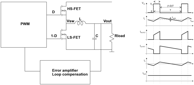
Figure 1: A synchronous non-isolated buck converter
Current Probe Around Conductor
A calibrated winding around the current-carrying conductor can be used to measure alternating current (AC). Combined with Hall-effect sensors, the frequency range can be extended down to DC. Current probes can be created as clamps [2] or Rogowski coils [3]. The clamp solution requires the probe winding to be completely around the current-carrying conductor, making these solutions too intrusive for some applications. Figure 2 illustrates three connection options. In case of this evaluation board the input and output of the converter were connected through long wires, making the use of a current clamp very easy. To measure the current in the inductor, on the other hand, required the lifting of one side of the inductor and adding the series loop.
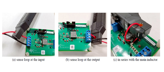
Figure 2: Current clamp connections in a low-current buck regulator evaluation board
For instance, a one-inch diameter wire loop represents approximately 100nH inductance. Adding this amount of inductance may be acceptable in series to the main switching inductor with a value of a few uH or higher. This limits this connection scheme to low-current regulators. High-current multi-phase regulators running at 300–1000kHz per phase tend to have inductor values in the same order as the inductance of the added loop, making the use of a 100nH extra inductance prohibitive. The input side of a buck converter is even more sensitive to extra inductance, since the current to be measured is discontinuous, so the loop must be placed outside of the first line of bypass capacitors (Figure 2a). Connecting the loop outside the first bypass capacitors of a non-isolated buck converter carries the advantage that the input ripple current is significantly diminished and the average input current is less than the load current. However, the added conductor to accommodate the current clamp not only increases losses, but the extra inductance also changes the dynamic behavior of the converter.
When it comes to measuring current sharing in multiphase converters, we need to measure the current separately in each phase, corresponding to the scheme in Figure 2c. Not only the loop for the clamp adds too much inductance, the space required for the loops and current probes for each phase also represents a significant challenge, making it very impractical to use current clamps for more than a couple of phases.
Using Rdson
Each of the components of the switching stage in Figure 1 has conductive losses, which can be utilized to measure current. For instance, both the high-side FET and low-side FET have a finite resistance, which creates a small voltage drop across the device when the device is turned on. The voltage drop is the complex product of the switch current and device impedance. By measuring the current from the voltage across the low-side FET, we obtain the current waveform during the ON time of the cycle. By measuring the voltage across the high-side FET, we obtain the current waveform during the OFF cycle.
When the switch is on, its resistance is low and therefore the main parasitic contribution to consider is from the series inductance of the part (see next Section). In a non-isolated buck converter the voltage drop across the high-side FET rides on the input voltage, what creates a challenge for the sensing circuit. The source of the low-side FET connects to the main return (ground), making it easier to measure. Utilizing the ON resistance of the switching devices will not add extra loss, but there are a few challenges and drawbacks. Figure 3 shows a typical waveform. We want to measure the few times ten millivolt switch-node voltage when the low-side FET is on. However, during the OFF cycle the switch-node voltage swings up to the input voltage. The ratio of the voltages during the ON and OFF cycles becomes greater as the input/output voltage ratio gets bigger as well as in designs with higher efficiency. The potentially big dynamic range creates a challenge for the measuring instrument. If we increase the sensitivity of the oscilloscope such that during the ON time we drive the A/D converter optimally, this will overdrive the circuit during the OFF period. Since the device under test (DUT) has low source impedance, a clamp circuit may help.
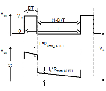
Figure 3: Switch-node voltage waveform and the waveform that can be utilized to measure current across the FETs ON resistance.
A second challenge is that in order to calculate the current from the measured voltage, we need to know the Rdson value. We can not rely on data sheet values, because the possible range of the FET Rdson resistance usually comes in a very big range; a range of 2:1 can be quite common. This calls for either calibration or correlation to other measured values, such as inductor current. Furthermore, Rdson has not only a large spread of its initial value, its temperature dependence is also quite high. Figure 4 shows a typical Rdson vs. temperature curve.
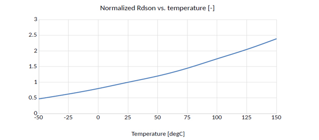
Figure 4: A typical curve showing the normalized temperature dependence of the Rdson of a FET. Based on Figure 3 of [4]
Lastly, the switch-node voltage has high-frequency transients near the switching edges, typically in the hundreds of MHz frequency range. This either has to be filtered out by analog or digital means, or this portion of the data has to be omitted from our data processing by applying a blanking window.
Using RC Network Across Inductor
One idea for current measurement is to shunt the inductor with a differential probe and attempt to infer current from the differential voltage measurement. All inductors in switch-mode power supplies have an inductance and a parasitic resistance. Without the parasitic resistance, the voltage across the inductor is given by the well known equation:with the current therefore given by:
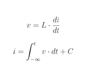
There are two obvious problems in that we cannot see the signal for all time and therefore we do not know the correct DC offset. The parasitic resistance helps here in that the transfer function of current with respect to voltage has a zero no longer at the origin, but there is a huge dynamic range difference between DC and the switching frequency leading to large amplification of low frequency noise in the measurement [5]. This causes the dynamic information in the waveform to be correct, but adds a low frequency wander to the measurement.
One technique that addresses this problem is to shunt the inductor with an RC network and to measure the voltage across the capacitor [6]. This technique requires matching of the R · C time-constant of the RC network with the L/R time-constant of the inductor and its parasitic resistance. The gain applied to this measurement is 1/R. This technique involves the soldering of components to the circuit with the time-constants hopefully matched.
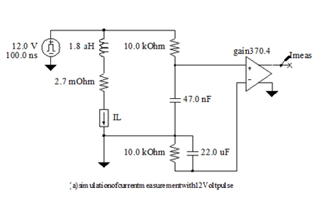
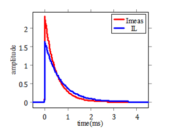
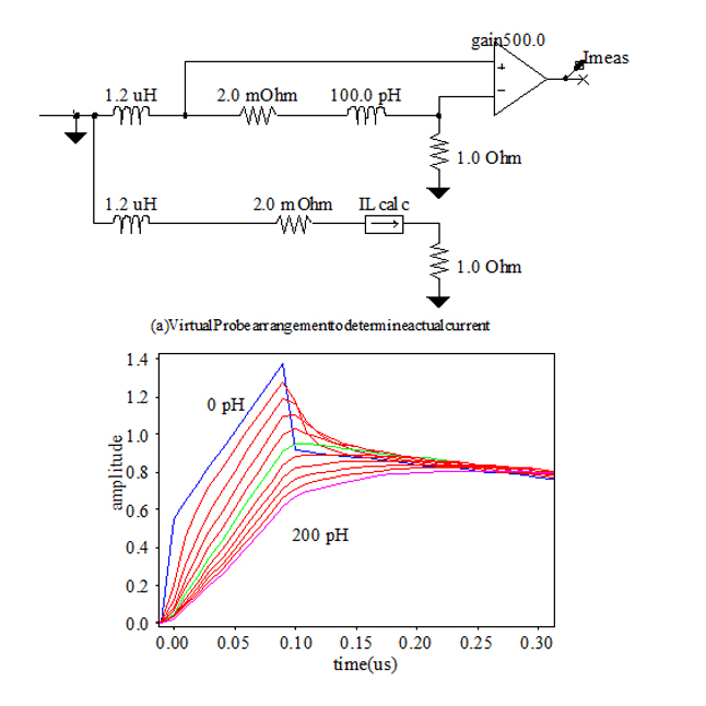
We are proposing an RC probe tip containing a similar circuit as proposed by [6] with some elements to reduce common-mode noise. We constrain the problem to roughly match the time-constants and use digital signal processing (DSP) to make the correction. In Figure 5a we see a simplified simulation schematic demonstrating the situation. Here we have an inductor with L = 1.8 µH of inductance and RL = 2.7 mΩ of parasitic capacitance. This is a time-constant of 666.7 µs. We have an RC probe tip with 10 kΩ of resistance and 47 nF of capacitance with a time-constant of 470 µs. We apply a gain of 1/RL = 370.4 to the measurement. The simulated resulting waveforms are shown in Figure 5b where see a large error between the measured and actual inductor current.
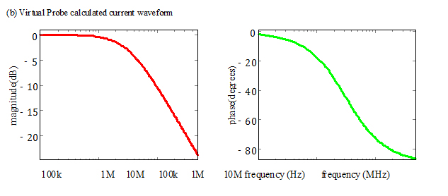
To provide a correct inductor current waveform, we use a technique called Virtual Probing [7][8]. In Figure 6a we have a virtual probe schematic. Virtual probing works by providing a schematic showing a circuit with a measurement probe placed where an actual measurement is taken (Imeas) and an output probe placed where the desired calculated waveform appears (Icalc). A solution is computed for a transfer function that converts the measured waveform at the measurement point to the waveform at the output probe location. We see the result of this processing applied to the measured waveform in Figure 5b to produce the calculated inductor current. The comparison of the calculated to the actual inductor current is shown in Figure 6b where we see that the two overlap. The magnitude and phase response of the transfer function for this processing is shown in Figure 6c and Figure 6d where we see only an approximate 3 dB of attenuation applied by the processing. Despite this small amount of mismatch, a high-gain, low-noise probe must be used for this measurement to get any kind of reasonable results [9].
(b) output waveforms showing time-constant mismatch
Figure 5: RC current probe waveforms
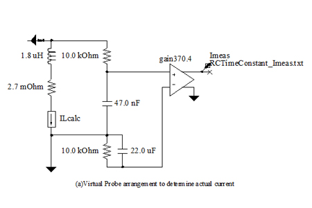
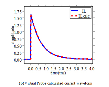
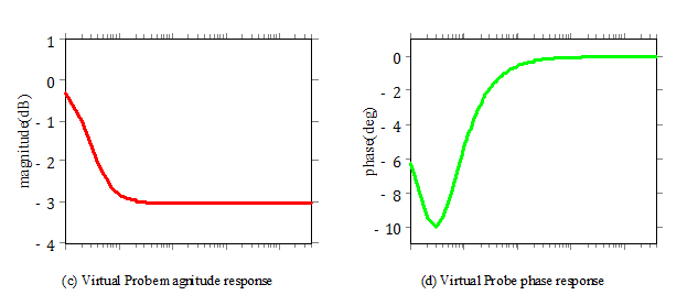
Figure 6: RC current probe Virtual Probing measurement technique
Using Sense Resistor
Another technique for current measurement involves using a sense resistor [10]. The sense resistor is a small valued resistor placed in series with the inductor, although it might be the parasitic resistance itself of a printed circuit board (PCB) trace or the pin of a part. The addition of such a resistor is invasive, if not already present and adds extra loss and can create current crowding problems in high-current regulators. That being said, it can be very accurate and low temperature coefficient (TC) resistors can be used for this purpose.
One might think that using a series sense resistor only involves measuring the differential voltage across the resistor and multiplying the voltage measurement by the inverse of the resistance. This is mostly the case, but as the reference points out, there is an often small parasitic inductance associated with the resistor. While small, it tends to have a very large effect on the measurement because the resistance itself tends to be very small.
(c) Virtual Probe magnitude response (d) Virtual Probe phase response
Figure 7: Sense resistor Virtual Probing measurement technique
In Figure 7a we show a virtual probe schematic showing a sense resistor with R = 2 mΩ and a parasitic inductance Lp = 100 pH. This is on the order of a reasonably expected parasitic inductance value. The virtual probe measurement point is the voltage measured by the differential probe with a gain of 1/R = 500 applied. The output probe is the inductor current IL in the schematic.
Various waveform outputs are provided in Figure 7b that show the pulse response of the system due to different assumptions about the parasitic inductance from 0 − 200 pH in 20 pH increments. This is shown because often the exact value of the parasitic inductance is unknown. Fortunately, switch-mode power supply inductor currents, especially under static load conditions, are saw-tooth shaped waveforms and one can see by examining Figure 7b that the correct value of Lp is fairly easily determined, especially if the processing for the correction is performed dynamically within a digital storage oscilloscope (DSO).
A parasitic inductance in series with a resistance as in this example causes a zero to appear in the transfer function. This zero is compensated for in the virtual probe transfer function whose magnitude and phase response are shown in Figure 7c and Figure 7d. Here you can see the corner frequency of (Lp/R)/(2 · π) ≈ 3.2MHz.
Measuring Current Sharing
Typical buck converter applications call for regulated output voltage. The output voltage is kept within the specified band against temperature, aging and load current variations by adjusting the duty cycle of the switches. This traditional feedback loop has many different implementations from full analog to full digital and many shades in between. Regardless of its implementation, the feedback loop carries the risk of instability. While the metric has been questioned in recent years, the de-facto standard way of assessing the voltage loop stability is to evaluate the small-signal open loop gain magnitude and phase in the frequency domain. When multiple phases are needed to supply the load current, additional feedback loop(s) are needed to make sure the phases share the current as planned (usually this means equal sharing). If the component losses and main parameters in the output filter were completely identical for each phase, a single control through the voltage feedback loop would be enough. In practical circuits, with the exception of current-mode control [11], component tolerances and unequal path impedance between each load’s output and the load require additional feedback loop(s) to equalize the current sharing. Figure 8 illustrates the output impedance seen be each of the phases in a six-phase regulator. Note that the variation across the phases is repeatable and it depends on the board layout and component placements.
DC path resistance (blue) and output impedance (red) at each of the six phases [mOhm]
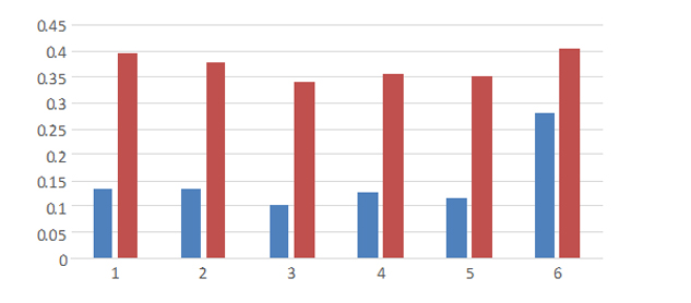
Figure 8: High-side plane resistance (blue) and output impedance magnitude at 100 kHz (red) seen by the phases in a six-phase DC-DC converter
Unfortunately in most converters the current-sharing loop is not accessible for the user; in off-theshelf digital implementations it is all in code, inaccessible to the customer. When at least parts of the current-sharing loops are accessible, a test setup is suggested to measure the open-loop gain with multiple excitation sources [1]. Without having access to the current-sharing loop elements to open it up and inject test signal(s), we can fall back on measuring closed-loop behavior. This would be equivalent to noninvasive stability measurement (NISM) [12] of the voltage control loop. The stimulus can be applied to the common output of the regulator, either by an external source or by relying on the varying activity of the real load circuit. These options are detailed in the following sub sections.
If we have a suitable voltage-to-current translator available, we can generate any load-current waveform by applying the selected waveform from a laboratory source to the voltage-to-current translator’s input and using the controlled current output to load the DUT. For relatively small currents and medium slew rates, we can use a bipolar or metal-oxide-semiconductor (MOS) transistor in emitter-follower mode and use it as a one-quadrant open-loop voltage-to-current converter. Some of the DC-DC converter evaluation boards have such a circuit placed on the board, ready for us to use. For high currents and very high slew rates the main challenge becomes the connection between the current source and DUT. Resistance and inductance of the connection will create voltage drops, reducing the voltage available for the active device, eventually setting a limit on the maximum current and slew rate. As an illustrative example, lets assume a 1 mΩ and 100pH connection impedance. Having a 100 A current step with 1000 A/µs slew rate, the resulting static voltage drop is 1 mΩ · 100 A = 100 mV and the dynamic voltage drop is 100 pH · 1000 A/µs = 100 mV, resulting in a 200 mV reduction of the available voltage for the active device. To overcome these limitations, custom fixtures can be created that minimize the voltage droop on the interconnect s [13]. Once we have a voltage-to-current translator, we can drive it to create any of the possible cases: small-signal, large-signal, swept-frequency sine wave or transient stimulus.
When an external stimulus injector is not available, or can not be connected to the DUT, we can analyze the current of each phase by utilizing the time-varying current of the load. The current sharing can be tracked as a function of time and each phase’s contribution can be plotted normalized to the ‘fair share’ value, which can be approximated as the average of the phase currents. If we have good control over the activity of the loading device, we can mimic any of the controlled cases: small or large signal sweptfrequency sinusoidal or small or large-signal transient stimulus. Parameters, such as repetition frequency can be swept and the sharing magnitude and phase can be plotted. As an illustration, later in this paper, Figure 12 shows a frequency sweep on a six-phase DC-DC converter and a time-domain capture at one specific repetition frequency. The current stimulus was created by the controlled activity of the loading device, generating current steps up to about 100A magnitude.
Current Sharing Measurements
Using a Python tool we are currently developing, we took current sharing measurements of a three phase supply. The measurements were taken using the RC probe tips connected to a Teledyne LeCroy APO33 active differential probe and were measured on a Teledyne LeCroy HDO8058 eight channel, 12 bit, 500MHz DSO. We took measurements of a three-phase, 30 Ampere and a two-phase, 90 Ampere supply. Both supplies are buck topologies each translating an input voltage of 12V to an output voltage of 1V. We also took measurements in-situ of an operating system using an aggregate six-phase converter.
The stimulus was applied using an Agilent N3300A electronic load for static DC current load and FETs located on-board the DC-DC converter evaluation boards for transient current generation. The gate of the FET is driven by a Teledyne LeCroy WaveStation 3162, 160MHz arbitrary waveform generator (AWG). The transient current is measured by the voltage across a sense resistor between the source of the FET and ground.
The current transients supplied to the evaluation boards can be of four forms:
- sinusoidal - The FET is driven in a class A amplifier arrangement with DC bias applied and a sinusoidal voltage swinging around the bias point at specified frequencies. The DC bias and amplitude are determined in a DC calibration step. In this mode, the amplitude limitations are mostly due to power dissipation of the FET and sense resistor. Usually, this mode can only be used for small signal measurements.
- pulse - the FET is driven by pulses that swing from a min to a max gate voltage at specified repetition rates. The duty cycle is held constant and specified. The min gate voltage is essentially the voltage required to mostly turn off the FET without resulting in undershoot and distortion caused by driving the FET fully off. The amplitude of the pulse is determined in a calibration step. In pulse mode, the amplitude limitations are usually not power dissipation limitations but instead are absolute drain current limits on the FET.
- burst - The FET is driven by pulse trains with a given period for a relatively short duration. The calibrationandvoltageamplitudesaresimilartopulsemode. Theburstsareeithermanuallytriggered by the software or externally triggered in the AWG by a trigger ready output of the oscilloscope. Using trigger ready, the burst is initiated by simply arming the oscilloscope for an acquisition.
- monitor - This mode does not stimulate the supply, but depends on external stimulus asynchronously sweeping through various frequencies. In this mode, the current sharing measurement must determine the stimulus frequency from the measured inductor current frequencies.
While sweeping or monitoring the DUT, measurements are made of inductor current sharing in two ways simultaneously: frequency-domain and time-domain.
In the frequency-domain, the discrete Fourier transform (DFT) is computed for each current waveform measured. The frequency of the transient stimulus applied is used to determine the DFT bin of interest. In the case of monitor mode transient stimulus, the bin containing the largest value (except DC) is used to determine the frequency. The magnitude and phase of the waveform at the frequency of interest is obtained. The phasor addition of all of the complex phase currents is added and the resultant magnitude determines the total current. The magnitude of each phase divided by the resultant magnitude determines the fraction of total current carried by the inductor. The difference between the phase of the inductor current and the phase of the resultant determines the measured phase.
In the time-domain, the inductor current waveform is optionally filtered to remove inter-phase switching transients. This filtered waveform is sparsed to reduce data readout. The filtered, sparsed data is then read out of the oscilloscope for processing. Each inductor current waveform is summed to produce the total current waveform. A threshold is applied (usually 90% of the maximum total waveform amplitude) and all points where the total current waveform is above the threshold are processed to form a sampling of fractional current carrying for each inductor. While these are time-domain measurements, the measurements are plotted versus frequency by finding the dominant frequency component of the waveform, excluding DC.
Statistics for each frequency are retained in the form of statistical data required to form the mean fraction and phase of the frequency domain data and to form a 95% confidence interval for estimation of the mean for repeated sweeps. The min, max, and mean time-domain data are retained.
One thing to note is the frequency-domain data only contains information on the fundamental of the transientportion. Thismeansthatthevaluemightbedifferentthantheamplitudeofthestimuluswaveforms in pulse or burst modes. The time-domain data contains both the static load current and the complete transient response with all frequency components.
Three Phase Supply Measurements
The measurement of a three-phase DC-DC converter is shown in Figure 9. In this measurement an attempt was made to measure the small signal current sharing by using a transient consisting of 1A of bias current and a 500mA amplitude sinusoid. A total of 10A of static current was utilized (9A pulled by the electronic load).
The frequencies were swept from 100Hz to 100kHz. The acquisitions were taken with lengths sufficient for 100Hz frequency resolution, but the sweeps were log-linear with a minimum of 10Hz resolution on the AWG. A flat-top window was utilized with the DFT to deal with measurements that were not bin centered. 1000 points per decade were specified, so the sweep resolution was very fine. The top four plots in Figure 9 are the frequency-domain measurements for the sweep. In Figure 9a, we see the fractional current sharing for each phase which should ideally be one-third. In Figure 9b, the phase relative to the total is shown. We see that the three phases track nearly perfectly in transient response up to a frequency of 10kHz, after which they deviate significantly. The first phase drops to 20% at 10kHz while the second two phases both rise to about 40%. One can also observe about 20◦ of maximum phase difference between the first phase and the second two. In Figure 9c, the fractional current is translated to a transfer characteristic in decibels, where 0dB refers to carrying one-third of the current.
The total current (in the frequency-domain) is shown in Figure 9d where we see a few noteworthy things. First, the total current amplitude is not 500mA as specified, but slightly larger. This can be attributed to the fact that the transient generation circuitry was calibrated to a DC current, not an AC current. Another interesting thing is the bump around 30kHz. This deserves further investigation but remember that we are driving transient current at the load and measuring inductor current, which can and will be different. We don’t necessarily care how precisely the current transients are driven, but this is a significant deviation. If precise control of total inductor current was desired (as opposed to load current), this would necessitate a frequency response calibration for the transfer characteristic between load current generated by the transient current generation circuitry and total inductor current. Finally, one can see that the current drops off after about 40kHz. This is due to the fact that the converter cannot even see the transient current generated at higher frequencies and the transient current is being drawn from capacitance in the system.
As a final note, in the four frequency domain measurements, there are 95% confidence interval shaded regions that are barely discernible around each trace. This measurement was taken overnight and the repeatability of the measurement shows that the estimation of the mean is near perfect. The only large
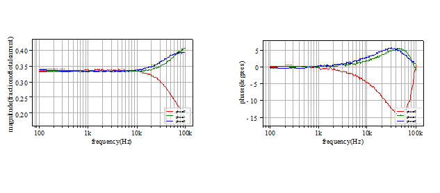
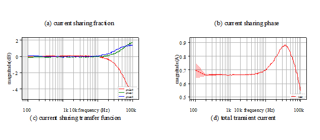
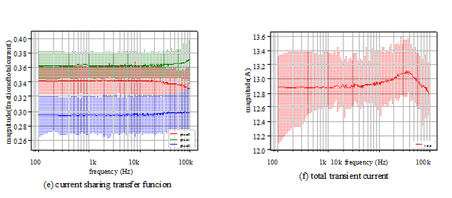
Figure 9: Three-phase small signal current sharing measurement sweep confidence interval is shown in Figure 9d at low frequency, which is attributable to the flat-top window applied.
The plots in Figure 9e and Figure 9f show the time-domain measurements. Remember, these are timedomain measurements, but are plotted versus frequency by determining the dominant frequency component. As such, these are time-domain measurements plotted versus essentially the stimulus frequency. In Figure 9f we see that the mean current draw is around 12.8A. It’s unclear that why there is so much deviation from the expected load of 10A static plus 0.5A transient expected (although the transient current deviation was already discussed) but it should be pointed out that the electronic load used was out of calibration. In Figure 9e and Figure 9f, the shaded regions represent min and max currents. The deviation is explained by the threshold used for the time-domain current determination: All currents over the threshold representing about 10% of the total current waveform is used leading to some variation. What is important to observe is the change in the min and max currents over frequency and any blips in the mean values. Here we see no such issues and we can conclude that the supply shares current well, at least from a small current transient response viewpoint, when considering the approximate 10A static load current over the entire frequency range.
Two Phase Supply Measurements
In Figure 10 we show a current sharing measurement using a two-phase converter. In this case we test the converter with a burst transient mode with 20 A of static current load and 64 A pulse amplitude. Each burst runs for 10ms, and is separated by about one second. The bursts are initiated by the software.
The sweeps are taken from 10 o 100 kHz with a 100 Hz nominal frequency step. Here, the dominant source of current is the transient current and we see in Figure 10b the total current dropping from about 90 to about 75 A over the frequency range. This is due to a combination of frequency response of the transient generation circuitry and decoupling of the output of the supply, but in any case is not too large of a drop.
By observing the mean and min/max values of the current sharing in Figure 10a, we can see many trouble frequencies where the min and max current sharing changes quite dramatically. The most troubling location appears in the vicinity of 91kHz where we observe the min and max current sharing ranging between nearly 20% and 80%, respectively.
The measurement was repeated by sweeping between 90 and 93 kHz in 10 Hz increments with a mean total current shown in Figure 10d of 94 A. In Figure 10c we see the trouble spot at a frequency of precisely 91.340 kHz, where for this sweep, the mean current sharing went to 40% on one phase and 60% on the other.
Because we are using an oscilloscope for these measurements, it was easy to set the scope and AWG for a repetitive measurement of the 91.340 kHz trouble frequency. In Figure 11 we show two oscilloscope screen shots of burst transient acquisitions. In each screen shot, the left two graticules show the measured inductor current with the first phase at the bottom in yellow and the second phase on the top an in red. Usually, these inductor currents would be a straight band across as the converter deals with the transient burst. In this case, we see quite a bit of low frequency wander due to the burst.
The right two graticules in each screen shot show zooms of the inductor currents where the zoomed area is indicated by bright bands in the waveforms in the left two graticules. The lower right graticule is simply the zoomed saw-tooth shaped inductor current waveforms with sharp discontinuities at the switch-node switching times. The upper right graticule is a filtered version of the inductor current where the switching has been filtered out. These are filtered with a linear phase, low-pass finite impulse response (FIR) filter
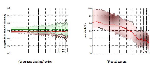
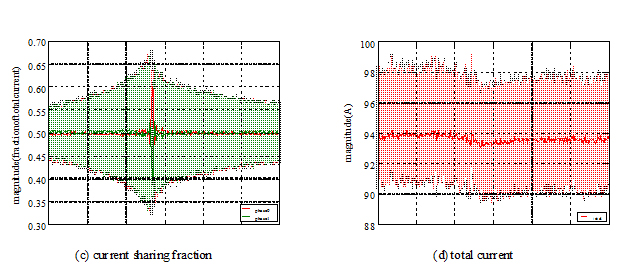
Figure 10: Two-phase burst mode current sharing measurement sweep
with a passband edge at 20 0kHz, a transition width of 100 kHz (i.e. a stopband edge at 300 kHz), and a stopband attenuation of 60 dB. The stopband edge is below the switching frequency. This processing was performed using built-in scope processing functions. The blue waveform corresponds to the first phase and the green waveform corresponds to the second phase.
In Figure 11a, we’ve zoomed in on a region of good current sharing. In the lower right graticule, we see the inductor current following the somewhat sinusoidal pulses in a piecewise manner. In the upper right graticule we see the filtered inductor currents overlapping. Each phase is carrying 10A of the 20 A static current on the low portion of the sinusoid and approximately 50 A of the approximate 100 A total current during the transient pulse.
In Figure 11b, we’ve zoomed in on a region of poor current sharing. In the lower right graticule, we see the inductor current following the transient pulses, but are offset from each other. In the upper right graticule we see the filtered inductor currents offset. Here, we see one phase carrying none and the other phase carrying all of the total 20 A static current. The first phase carries 80 A of the 100 A total current during the transient pulse. This shows a clear problem in that it’s possible for the first phase to trip its overcurrent protection, causing total system shutdown.
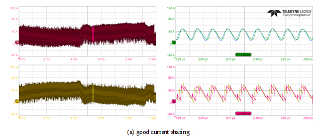
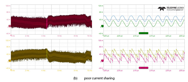
Figure 11: Time-domain burst mode current sharing measurements
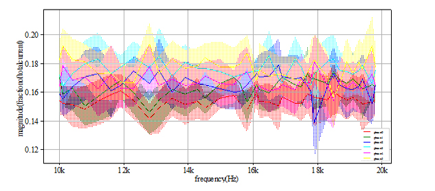
Figure 12: Six-phase monitor mode current sharing measurement sweep
Six-phase In Situ Current Sharing Monitoring
The device under test was a small computer card with multiple high-current supply rails feeding a big chip. The power rail measured here was fed from a six-phase DC-DC converter. Since the consumer chip was present, the stimulus was created by the controlled activity of the chip, creating large steps in current demand with controlled frequency and duty cycle. The frequency was swept through user-defined ranges and the current-sharing measurement operated in the monitor mode, where the software running on the oscilloscope automatically identifies the excitation frequency. Various settings of the six-phase DC-DC converter were tested. Figure 12 shows the quality of current sharing with a setting where at specific frequencies in the 10 − 20 kHz frequency range the current sharing was not sufficient. The plot shows solid lines, indicating the ratio of current in each phase. The correspondingly colored bands show the maximum/minimum range detected at the particular frequency. With ideal current sharing all six lines and bands were frequency independent with 1/6 value. Some deviation and negotiation is acceptable and it is inevitable under transient conditions. We can notice, however, that the solid blue line has a very sharp dip around 18 kHz. When the script controlling the chip activity was changed to hit that specific frequency repeatedly, the protection of the DC-DC converter was activated and it did shut down. Figure 13 shows the output voltage and the phase currents at the time of shutdown. There are eight plots in the figure. The upper left plot is the output voltage, shown with its full ±100 ms time window. The plot below is blank, reserved for a spare signal. The third and fourth plots below show the current in the first and second phases. The phase currents continue in sequence in the plots on the right: the top plot referring to phase 3, bottom plot referring to phase six. All phase currents are shown on the same ±1 ms zoomed horizontal and +130/ − 30 A vertical scales. The periodic fluctuation of currents is the result of the loading chip
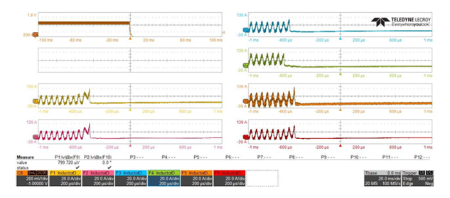
Figure 13: Six-phase converter shutdown during burst mode transient excitation
demanding periodically high and low currents. A close inspection shows that it is the fourth phase which runs at high peak values starting already at the left of the plot and it stops first. The other phases try to pick up the missing workload and their current signatures slope up sharply until they all shut down.
Sense Resistor and RC Probe Tip Measurement Comparison
Earlier in this paper, we discussed various ways to measure inductor current. The RC probe tip method is our preferred method as of now, but we wondered how well this compares to the sense resistor measurement. In Figure 14 we show a comparison. This measurement was taken by measuring the second phase in the three-phase measurement in Figure 9 simultaneously with a sense resistor. This particular evaluation board has a built in 3 mΩ sense resistor. The sweeps were retaken and only the phase of interest was retained in the plots.
The parasitic inductance was calibrated manually by adjusting the parasitic inductance specified in the dialog of the internal DSP processing component in the oscilloscope until, under static load conditions, the saw-tooth waveform for inductor current shape was correct, without the large overshoot (see Figure 7b). The tuning required a parasitic inductance of 500 pH at which time it essentially overlapped the measurement calculated from the RC probe tip. No further attempts at calibration were taken and the 3 mΩ sense resistor specified in the evaluation board schematics were used.
In Figure 7c we see that the current sharing computed for the RC tip is about 34% at low frequencies and the sense resistor provided just under 32%. The sharing mostly tracked, but came together at higher frequency. In Figure 7d we see that the phase tracks with an error under 2° across the entire frequency range. In Figure 7c we see the transfer characteristic where we see a 0.5 dB (or about 5%) difference at low frequency, improving at higher frequency. In Figure 14d we see the time-domain measurement, which is similar in difference as the frequency domain measurement in Figure 14a. These errors might be attributable to sense resistor tolerances (although the resistor is specified as 1%) or DC errors in the probe. If they were due to time-constant mismatch in the RC probe tip, then we would expect some deviation at low frequency, which we don’t see. In any case, all of these measurements show reasonable agreement.
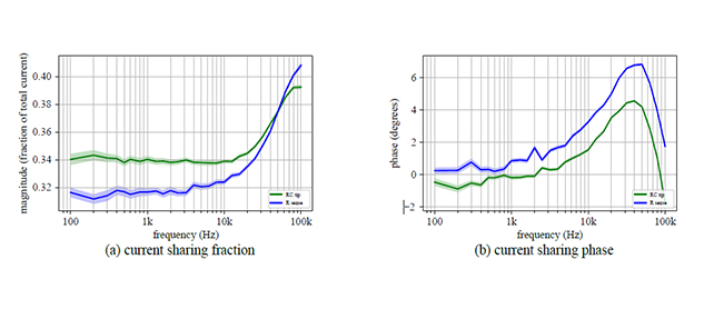
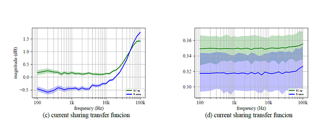
Figure 14: Sense resistor and RC probe tip current measurement comparison
Conclusions
InthispaperwehaveshownvariouswayshowinductorcurrentcanbemeasuredinDC-DCconverters. The proposed solution is based on commercially available hardware, replacing the often cumbersome and errorprone home-made setups. It was shown that with digital signal processing of the collected time-domain data, corrections can be made to compensate for unequal time constants between the inductor’s inductance and resistance and the RC time constants of the probes. Similar corrections are proposed to correct for the effect of series inductance of current-sense resistors. Using external, controlled stimulus, it was shown that the frequency-domain behavior of the closed current-sharing loops can be assessed and anomalies in the closed-loop response can reveal weak spots, which can be further analyzed by looking at the time-domain current waveforms. The solution is extended to automatically recognize the main signatures of current fluctuations, which makes it possible to analyze DC-DC converters with live loads.
Acknowledgements
The authors wish to thank Ted Steubing, Scott McCutcheon and Gene Whitcomb, Oracle, for their help with the measurements.
References
- Y. Panov and M. M. Jovanovic, “Loop gain measurement of paralleled dc-dc converters with averagecurrent-sharing control,” IEEE Transactions on Power Electronics, vol. 23, pp. 2942–2948, Nov 2008.
- http://teledynelecroy.com/probes/probeseries.aspx?mseries=426.
- https://en.wikipedia.org/wiki/Rogowski_coil.
- Advanced Power Technology, “Power MOSFET Tutorial.” Application Note APT-0403 Rev B.
- I. Novak and P. J. Pupalaikis, “A Generic Test Tool for Power Distribution Networks,” in DesignCon, UBM, February 2017.
- Linfinity, “A Simple Current-Sense Technique Eliminating a Sense Resistor.” Application Note AN7, July 1998.
- P. J. Pupalaikis, L. Jacobs, and S. Sekel, “Virtual probing and probe compensation,” February 2010. U.S. Patent 7,660,685.
- P. J. Pupalaikis, L. Jacobs, and S. Sekel, “Virtual probing and probe compensation,” May 2012. U.S. Patent 8,170,820.
- http://cdn.teledynelecroy.com/files/manuals/ap033-active-differential-probe-operators-manual.pdf.
- H. Zhang and K. B. Scott, “Switch Mode Power Supply Current Sensing.” http://www.linear.com/solutions/7646, November 2016.
- H. Zhang, “Voltage vs. Current Mode Control Current Sharing in a PolyPhase DC/DC Converter LTC3731, LTC3853, LTC3850.” http://www.linear.com/solutions/1014, December 2008.
- F. Hämmerle, S. Sandler, and T. Schuster, “Traditional and Non-Invasive Stability Measurements.” http://www.all-electronics.de/wp-content/uploads/2015/11/1-App_Note_Traditional_NoninvasiveStability_V2_0.pdf, 2015.
- E. Koether and I. Novak, “Transient Load Tester for Time Domain PDN Validation,” in EDICON, Microwave Journal, September 2017.