
Low Frequency Resistive Coupled Crosstalk
At low frequency, when the return currents spread out, they create a voltage drop distribution in the return plane due to the resistance in the plane. With a typical resistance in the return path on the order of 1 mΩ, and currents on the order of 100 mA, this is a voltage drop between one region of the return plane and another on the order of 100 μΩ, for example. This voltage drop, due to the low frequency DC currents on the plane, would appear as a voltage difference between the signal and local return plane on the victim path. It would show up at low frequency and last into DC. However, the magnitude of the resistively coupled noise might be orders of magnitude lower than the inductively coupled noise.
If there were a parallel gap in the return plane between the aggressor and victim traces, the impact on the inductive crosstalk would be small. However, the parallel gap would prevent DC currents from the aggressor’s return current from flowing under the victim trace and would eliminate the already small resistively coupled crosstalk.
The resistive crosstalk can be measured during the part of the square wave when the current is constant. Figure 7 shows the same measurement of the voltage on the victim trace with no gap between it and the aggressor signal during the entire square wave of current, but on a much higher resolution voltage scale. Note the switching noise that occurs at the edges of the square wave is just visible on this time base scale.
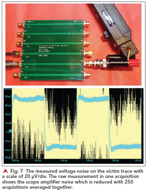
This is a very difficult measurement because the resistively coupled crosstalk is so small. With no averaging, the crosstalk is smaller than the 100 μV RMS amplifier noise of the Teledyne LeCroy WavePro HD, 12-bit scope. To reduce the random noise, we must average consecutive acquisitions, triggering the scope with the function enerator’s square wave. The random noise decreases with the square root of the number of averages, but the crosstalk synchronous with the function generator stays the same.
We see the very clear DC signature of the resistively coupled noise on the victim trace. Its magnitude is about 120 μV peak to peak. The small offset of about 20 μV is the DC offset of the scope’s amplifier. This 120 μV of resistively coupled noise for a peak-to-peak current of 120 mA corresponds to a coupled resistance in the ground plane of about 120 μV/120 mA = 1 mΩ of resistance, or the resistance in about 2 squares of ground plane for this board.
This 120 μV of resistive noise is due to the overlap of the return currents of the two conductors, roughly 1 in. apart, with 120 mA of aggressor current, passing through the 1 mΩ of overlapping plane resistance. This is the crosstalk noise we would want to eliminate with a split ground plane.
A Split Ground Plane Eliminates DC Resistively Coupled Noise
When we cut a gap in the return plane, there will be no DC current flow across the gap. There will be magnetic field coupling across the gap, which is why we still see significant mutual inductance coupling between the aggressor and victim across the gap. The gap has only a small impact on this noise.
However, we would expect there would be no resistively coupled noise on the victim trace on the other side of the ground plane gap. In Figure 8, the resistively coupled noise is measured with the same scale and averaging as the noise on the victim line with no gap. The noise floor of this measurement is about 10 μV. To this level, there is no measurable resistively coupled noise, a significant reduction.
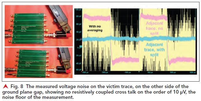
There is still inductively coupled switching noise that lasts for the rise time of the square wave, about 9 nsec. This noise is just barely visible with this time base of 100 μsec/div. It is the initial spike at the edges of the square wave.
It is this small amount of resistively coupled crosstalk that a gap in the ground plane would prevent. It keeps the DC currents, which will spread out from the signal paths, from flowing in the ground plane to induce a DC offset noise in the return path of other signals.
Generally, this amount of noise will be on the order of 100 μV, corresponding to 100 mA flowing through 1 mΩ of coupled resistance. In an ADC with a 5 V reference and 15-bit resolution (plus sign), 1 bit would be a voltage level of about 5 V/32,000 = 150 μV. The DC coupled ground plane voltage noise could contribute about 1 least significant bit level. Fluctuations in the 100 mA of ground currents, could be at the sensitivity level of a 16-bit ADC in some cases. It would be noticeable in a 24-bit ADC.
One solution to reduce this noise would be to isolate either the high current paths or the sensitive signal paths using an isolating gap in the return plane, parallel with the signal conductors, to make sure no signals cross this isolating gap. This is the problem solved by a gap in the return plane.
If there are 100 A of DC current flowing, the ground plane noise could be 100 mV or more, but other design considerations such as thicker copper, more ground planes, and placement of the VRM in proximity to the load must be considered.
While a gap in the return plane would dramatically reduce the resistively coupled noise on analog signals where voltage noise on the order of 100 μV was important, there is a more effective way of reducing this sort of common noise on sensitive signals that is also robust and does not run the risk of inadvertently having signals cross the isolation gap.
Differential Signaling Also Eliminates the Resistive Coupled DC Crosstalk
Most applications that are sensitive to 100 μV of low frequency noise involve measuring low level signals from sensors or microphones. An important design guideline when measuring these sorts of voltage sources is to use a differential measurement.
If the sensor itself generates a differential signal or even a single-ended signal, you would route a separate trace for both the high and low ends of the sensor, back to a differential receiver, such as an instrumentation amplifier. Even if the sensor is single-ended, the ground connection to the sensor’s low side could be connected at only one point, either at the sensor or at the input to the differential receiver, rather than both ends.
The voltage difference between the high and low side of the sensor is brought back to the input of the differential receiver, without using the ground plane, which might have the common DC voltage drop coupled noise in it. This separate dedicated low trace would not have the DC current of the return plane traveling in it.
This principle is illustrated in a simple experiment. A TMP36—a voltage sensitive temperature sensor—was used as the sensor. At room temperature, it generates a DC voltage of about 730 mV. It is a single-ended signal.
The output of this sensor was measured with a differential amplifier and a 16-bit ADC using the ADS1115. It was measured in two configurations, with the low side connected to the ADC using a common ground path, and with a separate return line connecting the low side of the sensor to the low side input of the ADC.
While these measurements were being made, a 1 Hz square wave of current was passed through the common return path. The common resistance was increased to accentuate the coupled noise. When the 100 mA of ground current was sent through the ground path, a noise level of about 2 mV was generated in the ground path from the sensor to the ADC. This voltage noise appears in series with the low level sensor voltage when the return path is used to connect the low side reference.
When the low side reference is carried in a separate, isolated trace, there is no impact on the differential signal from the DC noise in the return path. This result is shown in Figure 9.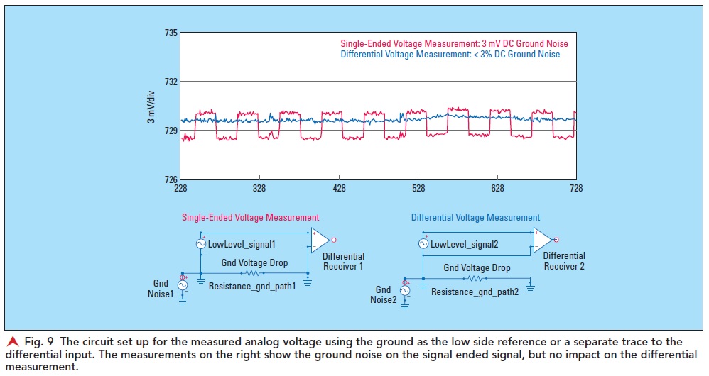
The differential signal path from the sensor to the differential receiver does not have the voltage drop of the ground plane in its path. The measured signal does not show any of the DC resistive crosstalk in its signal. This is the way to route sensitive analog signals, so they are not sensitive to very slight resistive crosstalk from low level signals.
Conclusion
The problem a split in the ground plane solves is reducing the very small low frequency resistive crosstalk of return currents which spread out. This typically arises at frequencies below 10 kHz and is equivalent of a common, shared resistance on the order of a few squares of sheet resistance, on the order of 1 mΩ.
If your application has very low level analog signals that must be routed across a board and might be sensitive to these low level sources of low frequency noise, a better solution is to use differential signal routing and a differential receiver.
The risk of adding a split in the ground plane to fix this very small problem is the possibility of higher bandwidth signals inadvertently crossing this gap. This can result in a pathological problem which will easily cause a board to fail in several ways.
Except in the simplest of boards, the risk from including a gap in the return path strongly outweighs the potential benefit. Carefully consider your engineering rationale to add a split in the ground plane, and to reduce risk, consider alternative solutions.