
It is a well-known fact that electromagnetic radiation can be emitted from the edges of printed circuit boards (PCBs) [1], [2]. When a current carrying via passes through two or more reference planes, an EM wave propagates radially away from the via within the cavity, as shown in Figure 1. It is guided by the respective planes; much like a water ripple will propagate radially away from a rain drop hitting a puddle of water. When the wave meets the PCB edge, the two reference planes form a slot antenna and will radiate noise with the potential to generate electromagnetic interference (EMI) to nearby equipment.
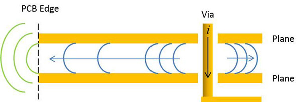
Figure 1 Simplified cross-section schematic of via passing through two adjacent plane layers showing edge emissions due to via induced EM fields between plane cavities.
Emissions can also occur when fringe fields from high frequency traces are routed too close to the edge of the PCB, or when unintentional currents are generated by power and ground noise, due to poor decoupling practices.
One way to mitigate this problem is to create a “picket fence” of vias around the perimeter of the PCB, as shown in Figure 2. They should be spaced at 1/8th of a wavelength (λ/8), and stitched to a strip of ground on every plane layer, as shown in Figure 3.
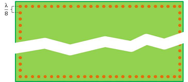
Figure 2 Top down illustration of a “picket fence” of stitching vias around perimeter of a PCB with spacing at λ/8.


Figure 3 Simplified cross-section view of via passing through several plane layers near the PCB edge with via stitching all plane layers to ground. When multiple vias are placed around the perimeter of the PCB, with a spacing of λ/8, a “picket fence” is created creating a short boundary condition which reflects the noise back towards the source.
The λ/8 spacing rule of thumb states that if the spacing between the stitching vias are less than or equal to 1/8th of a wavelength, the via fencing should appear to be the same as a short circuit, causing the propagating wave to be reflected back to the source [1].
If λ equals the velocity of propagation (v) in a dielectric medium, divided by the frequency (f), then it can be shown that via spacing (Svia) of λ/8 can be determined by Equation 1:
Equation 1
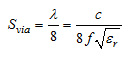
Where: c is the speed of light; and εr is the permittivity, or Dk of dielectric material.
Federal Communications Commission (FCC) Part 15, Class A and Class B define compliance limits for radiated emissions from digital devices. Class A limits refer to products that operate in a non-residential environment. Class B limits refer to products in residential environments, and are more restrictive than Class A. In Europe they have their own limits known as Comité International Spécial des Perturbations Radio Class A| B (CISPR Class A |B) and are slightly different than FCC.
At frequencies above 960 MHz, at 10 meters, the radiation emissions limits are 49.5 dBμV/m, for Class A, and 43.5 dBμV/m for Class B [3]. This means emissions must be less than 300 μV/m, for Class A, and 150 μV/m for Class B respectively. That’s not a lot to fail EMI tests.
In order to contain emissions above 960 MHz, the stitching via spacing must be on the order of 0.75” or less. A 50 mil pitch for via spacing will contain frequencies up to about 15 GHz.
Radiated emissions are mainly due to common signal noise escaping from apertures in the enclosure, or through cables leaving an enclosure. The primary source for common signal noise is from mode conversion from differential to common signals.
The major contributor to mode conversion is skew in differential signaling due to a difference in propagation delay between the positive and negative signal in a differential pair.
Skew is primarily caused by intra-pair asymmetry that can be caused by:
- Intra-pair length mismatch due to differences in trace lengths or through connector pins and receptacles. Right-angle connectors can be troublesome unless skew matching techniques were employed in the design of the connector.
- Non-symmetrical placement of return path vias near differential via pair when transitioning from one layer to another. In the same way, non-symmetrical ground pin assignment with respect to differential pins in connectors and IC packages can cause skew. In both cases the asymmetry creates a difference in loop inductance between the positive and negative signal.
- Fiber-weave effect in PCBs, where the fiberglass weave pattern causes a mismatch in differential propagation delay due to one trace of the pair being routed over mostly fiberglass bundle and the other routed over mostly resin.
Backplanes are notorious for having hundreds, if not thousands of vias, used for the connector pin headers that travel through the entire thickness of the PCB. They are also known for having long traces, which can exacerbate skew due to fiber-weave effect. Any mode conversion that happens when a signal travels from a source on one board, through the backplane, to the destination on another board, will launch common noise between the multiple plane cavities throughout the stackup. On a 34 layer PCB, for example, it is not unusual to have 16 plane pair cavities. So the potential for EM radiation from each cavity is quite high.
Via fencing stitched to ground along the perimeter is one way to contain the noise within the PCB. But one of the cost drivers for PCB fabrication is number of drilled holes and their drill diameters. On a large backplane, drilling holes around the perimeter, adds extra cost.
It is not uncommon for large Terabit systems to have large thick backplanes. For example, a 30” x 17” backplane with a stitching via spacing of 50 mils, that’s 1880 vias. If a second row of vias are also drilled beside the first row, and offset to fill the gap between adjacent vias in the first row, that’s 3760 vias. This will increase the cost even further.
Not only is there a dollar cost associated with via fencing, there is often penalties in terms of trace routing restrictions. By their very nature, the majority of equipment shelves, or chassis, have provisions for circuit cards to be plugged into card slots from the left side of a shelf to the right side. This often means the card slot connectors on the backplane are placed close to the edges of the PCB. Having two rows of via fencing, along with their spacing constraints, often compromise connector placement, and restricts trace routing between the connectors and the edge of the board.
Figure 4 shows an example of a portion of an inner layer of a large backplane. There are 12 columns of connectors for each of the respective card slots. Connector placements on the left and right side of the PCB are fairly close to the PCB finished edges, shown in yellow. As you can see, there are also traces routed between the respective connectors and both edges of the PCB. The other signal layers have similar routing along the edges.
In this design there was no room to include two rows of stitching vias along the left and right edges, and still be able to route traces there as well. Fortunately there was another solution, and that is called edge plating.
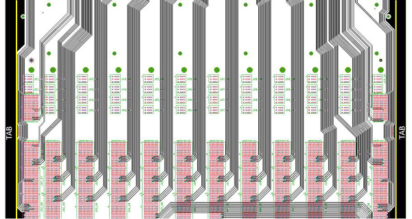
Figure 4 An example of a portion of an inner layer routing of high-speed differential pairs in a backplane
Edge plating, as the name suggests, is the process of plating the edges around the PCB. In my mind it is the best practice to prevent emissions from leaking out the edges of a backplane, and therefore it is my go to solution.
Here’s why.
During PCB fabrication, it is a simple process of pre-routing the outside edges of the board to final dimensions before the final plating process. It’s something that needs to be done anyways, so it’s just done before final plating rather than after. No additional fixturing is needed, and cost is minimal.
For successful edge plating there are some key design features that must be put into the artwork beforehand.
They are:
- Extending the copper on all layers past the finished edge of the board so plating can take hold. This can be seen in Figure 4 by the black copper fill extending past the yellow lines denoting the finished edges.
- Having small tabs spaced around the perimeter to keep the backplane attached to the panel during final plating.
- Adding stitching via fencing at exposed tab locations.
*Check with your particular fab shop for additional requirements and design guidelines.
Tab locations can be placed strategically during layout to mitigate any routing congestion. After final plating, a router or saw cuts the tabs away from the main panel. This leaves the edges exposed without plating. The double rows of stitching vias, at each tab location, prevent emissions from radiating out of the non-plated edge.
Referring back to Figure 4 you can see two tab locations, with associated stitching vias, were strategically placed in the open space between connectors on each side of the board. Also note that the routing of the traces needed to jog around the stitching vias. Had two rows of fencing vias been used around the whole perimeter, instead of edge plating, routing any traces between the connectors and edges of the board would have been limited. This would have severely impacted the board layout by adding additional layers and cost.
An example of an unplated tab and two staggered rows of stitching vias can be seen in Figure 5. The picture is from the same backplane I just described in Figure 4. The tab location is the right hand tab location shown in Figure 4.
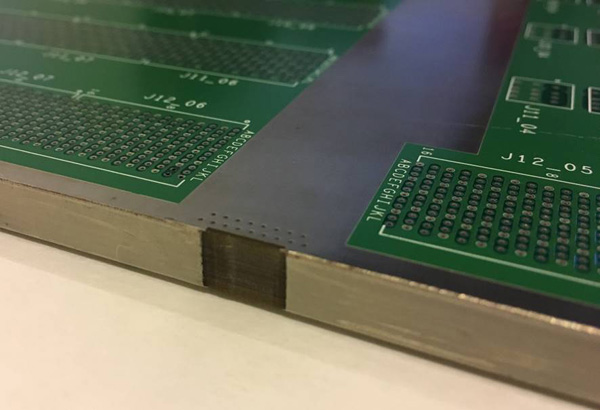
Figure 5 Edge plating example of a thick backplane showing unplated portion from the tab used to keep the PCB attached to the panel during final plating. The two staggered rows of vias behind the unplated portion are stitching vias to contain emissions.
Final Thoughts:
After reading this article, there may be questions, and doubts in your mind as to whether the actual emissions radiating from the edges of a backplane are enough to fail EMI testing? The short answer is I don’t know, and I don’t know if the answer can be easily answered universally without actually doing formal compliance testing of the final system with and without edge plating or via fencing.
To put it context, large terabit routers and data switches can be composed of a dozen or more line cards with different functionality, all switching asynchronously. Everything from Gigabit Ethernet to 40 Gigabit optical line cards can be plugged into the same shelf and backplane. EMI testing for such a large beast takes considerable resources, time and money.
EMI compliance testing at the system level usually requires a system to be built from the intended contract manufacturer, rather from first lab proto-types. This is a very expensive outlay in capital development cost, not to mention custom software required to exercise the system to emulate real live traffic.
Finally actual EMI compliance testing usually occurs off-site in an open field testing facility which is costly to ship equipment and do the testing. Testing two different systems requires at least two different backplanes to be designed, built and installed into two different factory built shelf mechanicals. Then there is the added cost of tear down, set-up, and repeating the testing a second time.
Even if you went through all that effort, and the system passes without edge plating, it doesn’t guarantee the system or backplane will pass in the future testing when new hardware is designed, or the same backplane is reused in another product configuration.
Unlike circuit cards that plug into the shelf, a backplane is the heart of the system. Once installed into the field, it stays there for the life of the product. During that lifetime new circuit cards get designed all the time and sometimes the speeds on the serial links can double and maybe quadruple.
As an example, a new system being designed today may be required to have all of the serial links run at a conservative 10GB/s. But the backplane needs to be 28GB/s ready for NRZ (non-return to zero) signaling and 56 GB/s PAM-4 (pulse amplitude modulation) after that. Since digital signals are composed of a series of odd harmonics over and above the fundamental frequency, there will be frequencies well above FCC limit at 960MHz.
Silicon technology shrink is always pushing edge rates faster and faster. At 28 GB/s, the fifth harmonic of the 14 GHz Nyquist frequency is 70 GHz! That will require a stitching via spacing of 10 mils which is not practical for thick backplanes of 300 mils or more because of drill aspect ratio.
At the end of the day, no company is going to go through all this effort and risk just to save the small cost of via fencing or edge plating. So we tend to just suck it up and do it. If you buy into this argument and want to prevent any EM energy from radiating from the edges of a backplane, then edge plating is the only practical cost effective solution and lets you sleep at nights.
References:
- W. Lindseth, "Effectiveness of PCB perimeter Via fencing: Radially propagating EMC emissions reduction technique," 2016 IEEE International Symposium on Electromagnetic Compatibility (EMC), Ottawa, ON, 2016, pp. 627-632. doi: 10.1109/ISEMC.2016.7571721
- H. Chen, J. Fang “Effects of 20-H Rule and Shielding Vias on Electromagnetic Radiation From Printed Circuit Boards”.
- P.Donohoe, “EMC STANDARDS” Mississippi State University Course Notes, EMC Requirements ece4323EMCreq.pdf