
The Voltage Regulator Modules (VRMs) are a vital part of any hardware design and critical to system-level power integrity analysis. When available, VRM models provided by the vendors offer a reasonable starting point for a power integrity design analysis, assuming the model properly represents the output impedance. However, these should not be used for design sign-off. The resistor-inductor (R-L) model is typically the most common SPICE representation for the ideal VRM small-signal passive model. Ideal VRM models in SPICE can sometimes provide reasonable first-order approximations for circuit behavior [1]. However, there should be caution in using these models without verification by making measurements. R-L models only include one of six noise sources in a VRM, the output self-impedance. The input self-impedance, power supply rejection ratio, reverse transfer, input noise current, and output noise current are all important sources of noise that are missed in an R-L model. [2] Furthermore, the small-signal passive model also gives up the dynamic impedance of the VRM due to changes in the load step current.
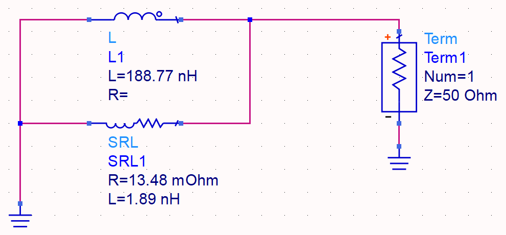
In this paper, the Analog Devices Inc. (ADI) LTM4650A micro-module with an internal inductor [3] is examined, comparing the generated small-signal passive model from LTpowerCAD [4] to a measured model using the LTM4650A evaluation board. This evaluation board, the DC2603A-A, contains a single LTM4650A with either a single phase or dual phase output configuration. In this measurement, the LTM4650A has two separate outputs (single-phase), with the measured output of one phase set to 1.5V. The LTpowerCAD schematic of the evaluation board is shown in Figure 1.
The setup shown in Figure 1 was used to generate the output impedance result shown in Figure 2. This setup also reflects the changes made to the LTM4650A EVAL (DC2603A-A) to remove a 100uF, 1210 package size capacitor, which was necessary to allow a probe point with the Picotest P2102A-1x 2-port probe [5].
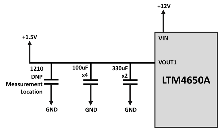
Figure 1. LTpowerCAD DC2603A-A Simplified Schematic
Figure 2 shows the output impedance plot from LTpowerCAD over the frequency range of 5Hz to 50MHz. The peak impedance value is 10mΩ at 9.988kHz. Additionally, the low-frequency impedance decreases significantly as the frequency decreases, reaching approximately 118uΩ at 100Hz.
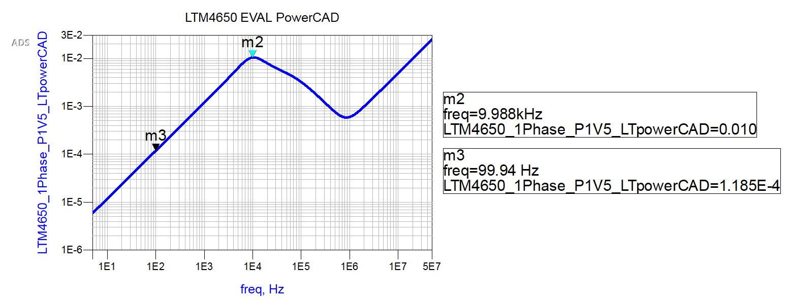
Figure 2. LTpowerCAD Impedance Graph
As shown by the output impedance results in Figure 2, there appears to be a linear approximation of the VRM at a low frequency from 5 Hz to 1kHz. This would indicate a sub-100 uOhm impedance that includes Rdson and DCR of the internal inductor and the non-linear elements of the control loop. The control loop parameters of Vramp, the sawtooth voltage ramp feeding the pulse width modulator (PWM) comparator, have a significant role in the output resistance of a VRM. These two elements are non-linear and vary based on the VRM operating conditions. As load current changes, so does Vramp. An accurate definition of these parameters is necessary to create a simulation model that best shows these characteristics [7]. Equation 1 demonstrates the relationship between the output impedance and Vramp. Figure 3 shows a graph of Vramp from 0.01V to 1000V and the non-linear output impedance as a function of Vramp.
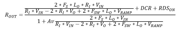
Equation 1. Output impedance of a non-isolated synchronous buck topology VRM [7]
Figure 3 clearly shows a non-linear result in the output impedance as the Vramp changes to meet the demands of the load. This nonlinearity is not caught in LTpowerCAD’s small signal passive model, which is only centered around a single point for Vramp.
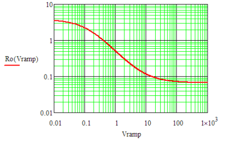
Figure 3. Vramp vs. Rout as a function of Vramp [7]
Figure 4 depicts the equivalent output circuit SPICE created by LTpowerCAD to represent the VRM on the DC2603A-A eval. This is the VRM equivalent SPICE model seen in the graph in Figure 2. Keysight PathWave ADS allows the user to plot SPICE models and measurements to enable the user to make comparisons.
A measurement was made on the LTM4650A DC2603A-A EVAL [8] design to validate the predicted output impedance reported by LTpowerCAD. A single-phase of this VRM was measured using Omicron’s Bode 100 VNA, using a P2102A-1X probe with a J2113A Semi-Floating Differential Amplifier [9]. The measured VRM phase matches the setup shown from LTpowerCAD in Figure 1. A 0.105 Ohm load resistor was connected to the VOUT1 port to provide a load current of around 14A.
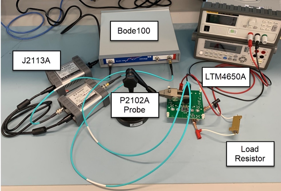
Figure 5. Lab Simulation
In Figure 6, the light blue line is the short measurement on a 5 oz copper substrate to demonstrate the measurement system noise floor after calibration. The magenta line is the VRM measurement at the depopulated capacitor pad with a 0.105Ω load resistor attached to the VRM. There is a slight increase in the impedance of the measurement below 10Hz not seen on the known DUT or noise floor. This is likely caused by human error in the measurement between 5Hz and 10Hz but does not impact the measurement above 10Hz. The dark blue line is the measurement of a known 330 uOhm resistor. This known measurement is used to confirm the calibration of the test setup. In Figure 6, the measurement results show similarities with the equivalent circuit seen in Figure 2.
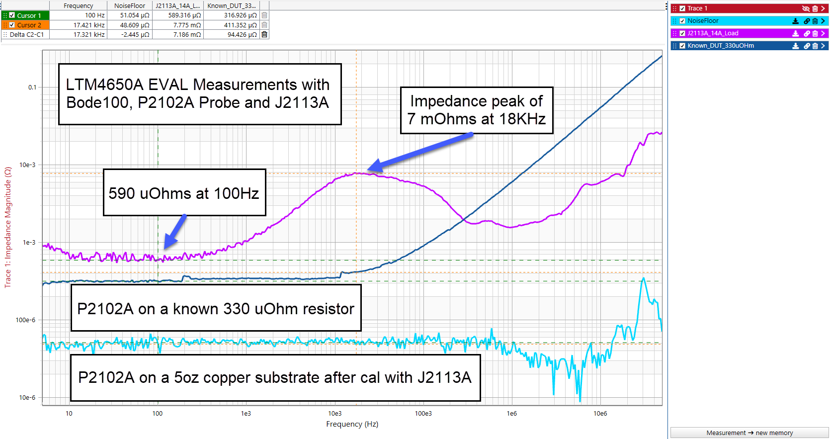
Figure 6. Measurement Results of the DC2603A-A evaluation board
Figure 7 shows the overall equivalent circuit created from Figure 4 for the measurement shown in Figure 6.
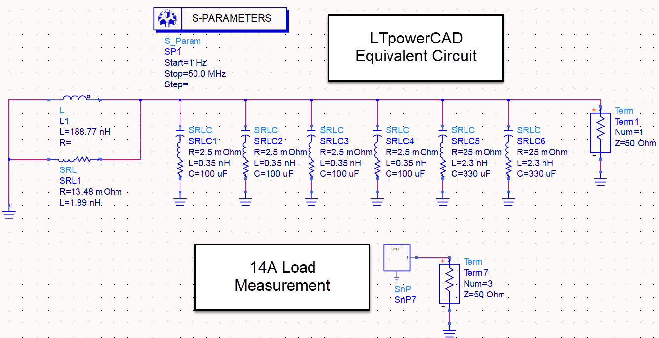
Figure 7. Keysight ADS Simulation Model for LTM4650A Eval
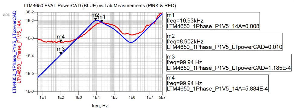 Figure 8. ADS Simulation Results Comparing LTM4650A LTpowerCAD to Lab Measurements
In Figure 8, the two models are in reasonable agreement at frequencies from 500Hz to 50MHz. However, from 5Hz to 500Hz, there is a stark divergence in each model. Markers m1 and m2 show the differences between the peak impedance measurement and LTpowerCAD simulations. The LTpowerCAD peak impedance is 10mΩ at 11.21kHz, whereas the measured value is 8 mΩ at 19.93kHz, a 9kHz difference in frequency. The 2mΩ impedance amplitude difference and shift in frequency between LTpowerCAD and measurement could be due to the inductive difference in the feedback compensation network in the control loop of the VRM [10]. It is important to note that the model is the typical case, and the measurement is at an unknown state between best and worst case. There are also differences in the actual capacitance, ESR, and ESL seen by measurement versus what was used in LTpowerCAD. This observation further emphasizes the importance of having good fidelity passives models. Markers m3 and m4 show a much different result, with a significant divergence before 100Hz that begins at 5Hz. LTpowerCAD only starts its graph at 100Hz; anything lower than that is extrapolation. At 500Hz and lower, the measured model shows a more accurate representation for the Rdson, DCR of the internal inductor, and loop gain of this VRM. Whereas with the LTpowerCAD model, these model parameters are not included. The higher output impedance may also be impacted by the series place resistance between the measurement point and the regulators regulation/sense point.
Figure 9 shows the fitted SPICE model created to fit the 14A load measured model, in red, up to a frequency of 100KHz, as this is roughly the frequency of just the VRM effects on the impedance. The capacitor models are created from the values seen in Figure 1 for capacitance, ESR, and ESL. At frequencies typically greater than 50kHz, the printed circuit board (PCB) effects start to impact the output impedance. Figure 4 shows the LTpowerCAD equivalent circuit model, which includes two inductors and a resistor. This is plotted in blue in Figure 9. The fitted model finds values for these inductors and resistors that best match the measured model using the ADS tuning tool. A second resistor is added before the two inductors and resistor provided by LTpowerCAD. This is to best model the DC resistance seen in the measurements.
A resistor is added that models the impedance from DC to 200Hz, where the inductance of the VRM starts to have an impact. For the 14A load fitted model, the resistance chosen is 650 uΩ, which is noticeably higher than the 100Hz measurement of 590uΩ. This is due to the 100Hz impedance being lower than the average impedance from DC to 200Hz. The new inductors are 124.59nH and 31.65nH. The resistance of the 31.65nH inductor is set to 9.84 mΩ. This compares to Figure 4, which has an inductor of 188nH and 1.89nH, with the 1.89nH inductor’s impedance being 13.48 mΩ. These show significant differences between the LTpowerCAD model and the measured models.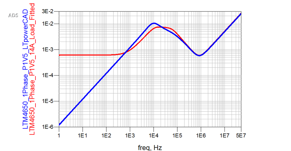 Figure 9. Fitted SPICE Model between LTpowerCAD and Measurement
In Figure 10, the percent error between LTPowerCAD and the measurement is used to quantify the differences between these two models. A purple limit line is shown at a 10% error to highlight the frequencies that are above or below this value. A cyan shading area at 100KHz and above shows the area where the PCB effects on the PDN take effect. At 100Hz, the LTpowerCAD model error is 418% with the 14A load! This is potentially due to the Ri, Vramp, Rdson, and the DCR values in the LTpowerCAD model. The models converge slightly better at 5KHz, 41.46% percent error between LTpowerCAD and the measurement. 5Hz is roughly in the middle of the primary inductance curve in the measurements and LTpowerCAD model. A reasonable expectation based on engineering judgment would suggest a value of 10% or less error. In this case, the 41.46% error is the smallest error between the LTpowerCAD small-signal passive model but still seems excessive.
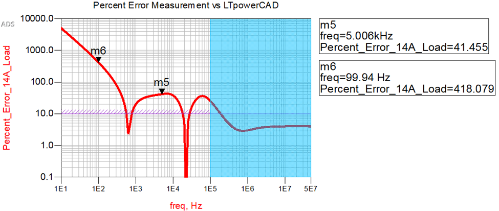 Figure 10. Percent Error between Measurement and LTpowerCAD
LTpowerCAD uses a small-signal passive model to generate VRM SPICE models. Without a measurement characterization of the evaluation board, these model differences would have been missed, and the power integrity system-level simulation model would have had multiple discrepancies. Vendor models can help start a design, and LTpowerCAD is a helpful tool that provides valuable information to the designer; however, vendor models are not always accurate or even correct. Therefore, designers should trust and verify their models with measurement.
Large-Signal Model vs. Small-Signal Model
Typically, there are two major categories for switching circuit models, average models and transient switching models. Switching devices are either in an ON or OFF state; therefore, to simulate such a circuit, the switching action must be averaged to generate a small-signal passive model. Output impedance, open-loop phase gain, and input impedance are simulations that can be performed with average modeling. However, average modeling only supports some transient analyses. The major drawback is that ripple, spikes, gate charge, and instantaneous switching loss are not available [11]. Whereas, with the Sandler State-Space Average model in Keysight PathWave ADS, a small-signal and large-signal model can be created for the LTM4650A VRM, where the PCB effects can easily be included to understand your power integrity system. Further, this VRM model allows simulation in discontinuous conduction mode (DCM) and continuous conduction mode (CCM). At the same time, including the ability to model linear and non-linear responses. The Sandler State-Space Average VRM model for the LTM4650A is shown in Figure 11. With a large-signal model, the non-linear responses can now be included, which are not part of the small-signal passive model from LTpowerCAD. To create this model, only a few additional measurements must be made on the DC2603A-A eval to characterize the LTM4650A VRM. As shown in Figure 11, the nonlinear large-signal response of the switch node, output ripple, and inductor current is captured along with the small-signal output impedance response.
The Sandler State-Space model provides a much higher fidelity model that allows designers to emulate better the nonlinear large-signal behavior found in VRMs. It also includes the five noise characteristics missing in the R-L model. The small-signal passive model accounts for the circuit behavior around an operating point. It linearizes the nonlinear behavior around a specific DC operation point, yet the behavior of electronic components, such as diodes and MOSFETs used in VRMs, are nonlinear. Using a small-signal passive R-L model can be highly linear, which does not accurately represent a switch within a VRM. This can cause significant discontinuities in the circuit node voltages that will not be included in a small-signal model. Many designers today are using small-signal models when they should also be using large-signal models. With small-signal models, you cannot accurately model the nonlinear response that occurs in a real system. Instead, the nonlinear response can accurately be simulated with a large-signal model that includes the PCB parasitic effects.
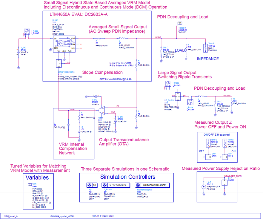
Figure 11. Sandler State-Space Average Model Schematic for LTM4650A EVAL: DC2603A-A
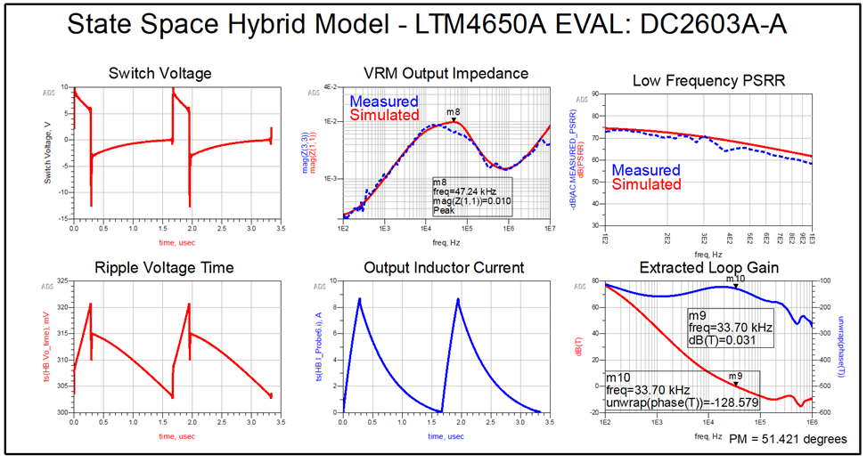
Figure 12. Sandler State-Space Average Model Results for LTM4650A EVAL: DC2603A-A
Figure 13 shows the percent error between the measurement and Sandler State-Space Model in red, and the percent error of LTpowerCAD vs the measurement in blue. At 100Hz, the difference between LTpowerCAD and the measurement was 417%. With the Sandler State-Space Model, the error between the model and measurement is only 4% at 100Hz. At low frequency values, up to a 30KHz the Sandler State-Space Model is always below 10% error when compared to the measurement. At higher frequencies, the LTpowerCAD model has a lower precent error than the Sandler-State Space Model, however this is in the cyan colored region where the PCB board effects start to influence the PDN. Adding the evaluation board artwork to the Sandler State-Space Model would result in higher accuracy at >30KHz, however this artwork was not available at the time of writing.
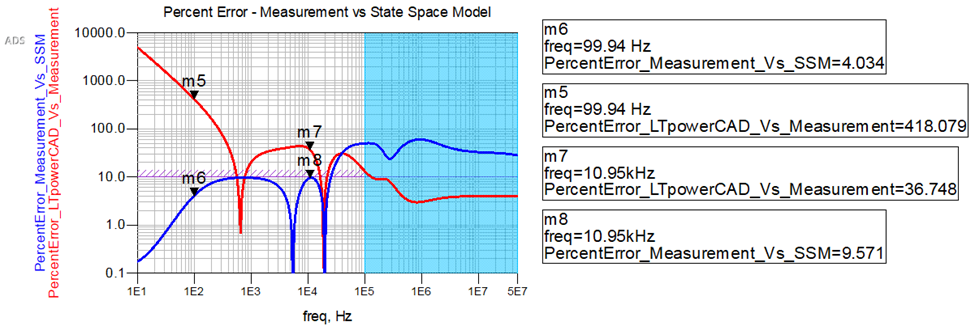 Figure 13. Percent Error Between Sandler State-Space Model and Measurement
Conclusions
While practical and a mainstay in power electronics design, the small-signal passive model has its downsides. By setting up around a DC point in the small-signal passive model, artifacts of the overall regulator in nonlinear operation are certainly removed and not present in the simulation. All the regulator's behavior will be seen when measured and tested in a real-world system. Therefore, to have a high-fidelity power system model, it is imperative to accurately represent all the design elements, including the PCB parasitic effects. Here it has been shown that a small-signal passive model will only provide you a limited fidelity in AC analysis and that it is essential that system-level power integrity analysis looks at both the small-signal and large signal models for system-level design signoff.
To drive home the criticality of designing our systems in this manner, we can reference an article by Steve Sandler [1], where he discusses how many low-power circuits are hyper-sensitive to power supply noise. If the simulation model is not accurate, potential design flaws of the model or errors may not be caught until the production cycle. Designers must take their own measurements so that the designer can verify and trust the model.
Lastly, to reference a quote from Eric Bogatin about signal integrity problems, that exact quote can be said similarly for power integrity problems. In other words, “there are two types of engineers, those who have power integrity problems and those who will.”
Acknowledgements
I want to thank Ben Dannan (Northrop Grumman), Steve Sandler (Picotest), and Jim Kuszewski (Northrop Grumman) for all their time and comments while working on this paper.
References
[1] Sandler, S. (2017). Designing Power For Sensitive Circuits. Signal Integrity Journal.
[2] Sandler, S. (2019). Why Full VRM Characterization is Essential. Signal Integrity Journal.
[3] LTM4650. (2022, 03 27). Retrieved from www.analog.com: https://www.analog.com/en/products/ltm4650.html
[4] LTpowerCAD and LTpowerPlanner (2022, 05 10). Retrieved from www.analog.com:
https://www.analog.com/en/design-center/ltpowercad.html
[5] Picotest P2102A-1X 2-Port Transmission Line PDN Probe (2022, 05 10) Retrieved from
www.picotest.com https://www.picotest.com/products_PDN_Probe.html
[6] Sandler, S. (2017). Measurement Based VRM Modeling https://www.picotest.com/downloads/Measurement-Base-VRM-Model-Tutorial-Final-2017.pdf
[7] Sandler, S. (2017). Characterizing and Selecting the VRM. Design Con 2017.
[8] DC2603A-A LTM4650AEY Demo Board - https://www.analog.com/en/design-center/evaluation-hardware-and-software/evaluation-boards-kits/dc2603a-a.html
[9] Picotest J2113A Semi-Floating Differential Amplifier - Ground Loop Breaker - (2022, 05 10) Retrieved
from www.picotest.com https://www.picotest.com/products_J2113A.html
[10] Sandler, S. M. “The Inductive Nature of Voltage-Control Loops” EDN - https://www.edn.com/the-inductive-nature-of-voltage-control-loops/
[11] Sandler, S. M. (2018). Switched-Mode Power Supply Design with SPICE. FaradayPress.
[12] Dannan, B., & Sandler, S. (2021). Calibrating the 2-Port Probe for Low Impedance PDN Measurements. Signal Integrity Journal.
[13] Dannan, B., Kuszewski, J., McCaffery, W. et al. (2022, July 7) Improved Methodology to Accurately
Perform System Level Power Integrity Analysis Including an ASIC die. Signal Integrity Journal.
[14] Omicron Lab Bode 100 VNA - https://www.picotest.com/products_BODE100.html
[15] Picotest PDN Cables - https://www.picotest.com/pdn-cable.html
[16] Picotest J2111A Current Injector - https://www.picotest.com/products_J2111A.html
[17] Barnes, H. (2021). Power Integrity Target Impedance Says it All, Power Delivery is AC not DC. 14th Annual Central PA Center for Signal Integrity Symposium, (pp. 1-54). Harrisburg.