
Over my career I’ve had the opportunity to spend a lot of time optimizing systems. Unfortunately, I’ve seen many systems fail to live up to expectations, and it was almost always due to an implementation failure at the breakout region (BOR).
A good example of this was a design at a network company that uses our Flyover® cable system. The channel performance was degraded, and the overall loss was double what was expected. We determined that the root cause for this loss was that the BORs were not using the tuned design we provided. It also was degraded by their ASIC BOR. These were really poorly done; for example, a 100 ohm transition was only 80 ohms. We’ve also seen this with other customer designs where the breakouts in the channel aren’t optimized. With our low loss Flyover cable solutions, this becomes even more important (see Figure 1).
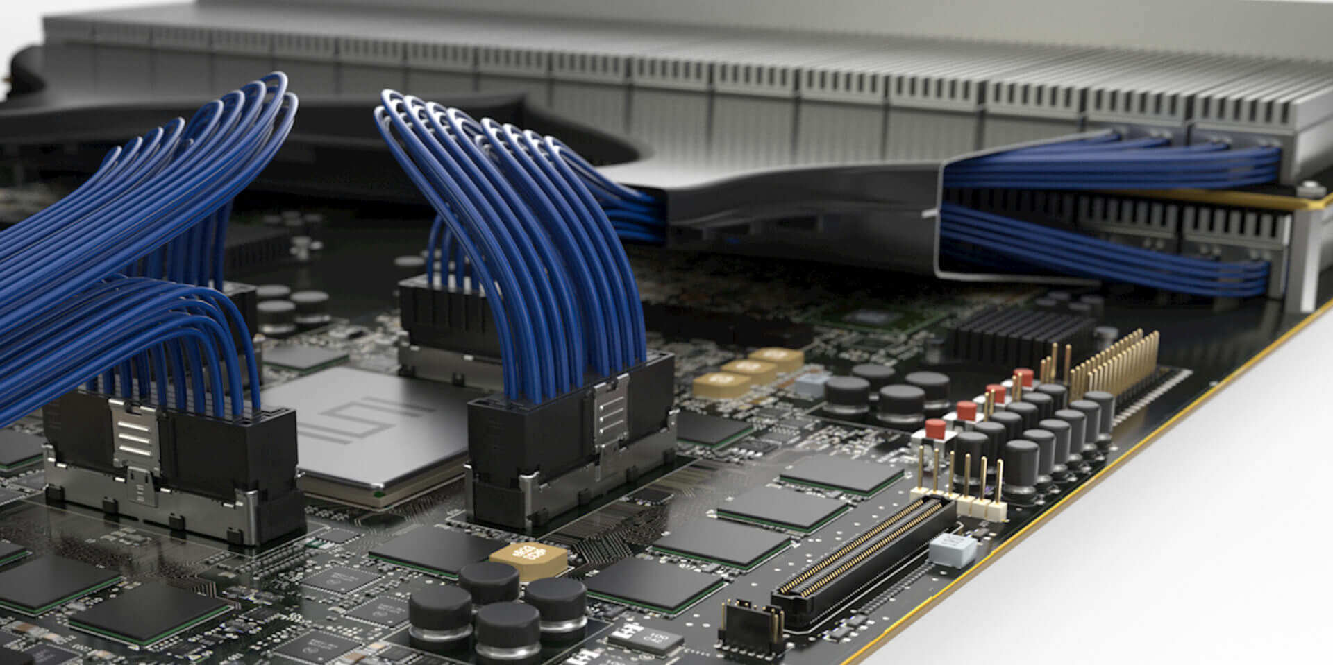 Figure 1: Example of a Samtec Flyover cable that routes signals through ultra-low skew twinax cable.
When using this type of cable system, the end-to-end loss is significantly lower, often 50% or even 35% of what was originally in the channel. Typically, excess loss is concentrated between the two connectors and their BORs. Once the loss is minimized, the reflections caused by a poor breakout are no longer attenuated by the channel loss.
With a poor BOR you can have a lot of ringing in the insertion loss due to undamped reflections (see Figure 2).
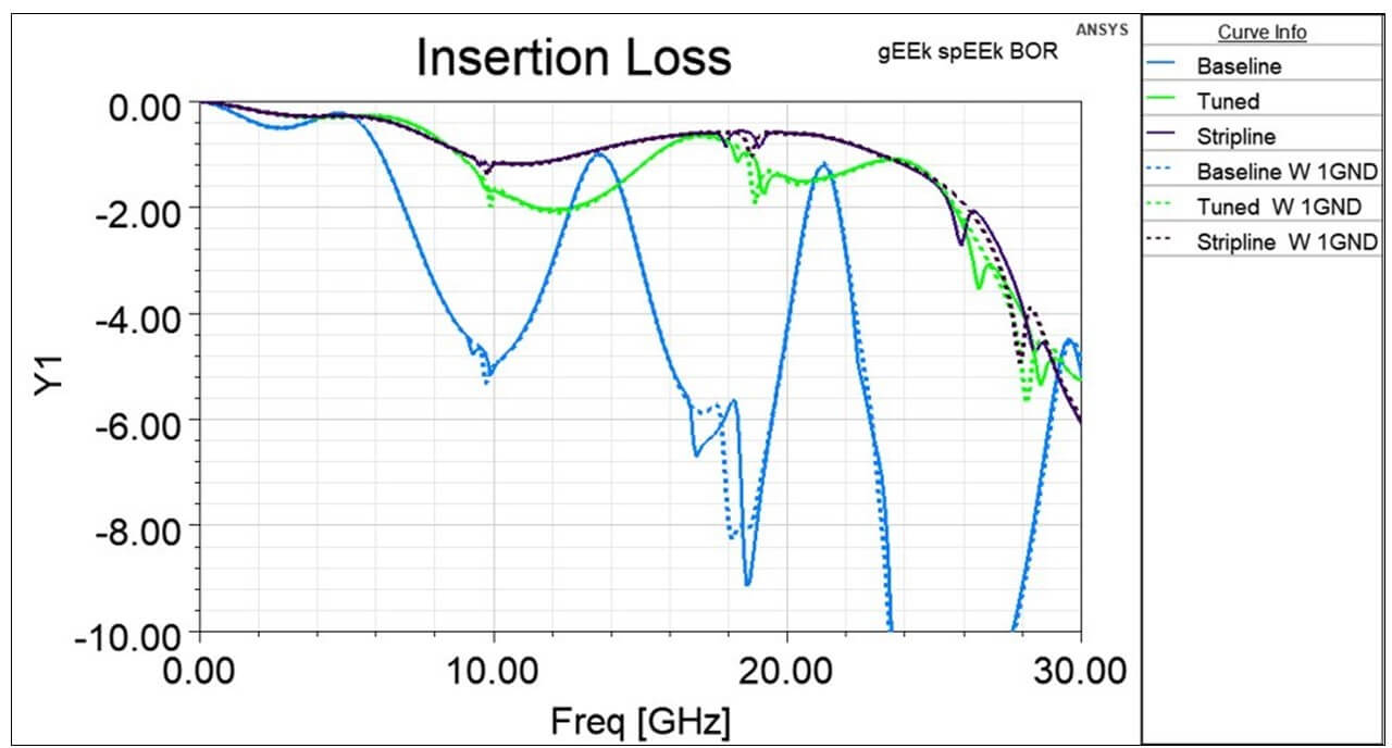
Figure 2: This graph illustrates why BORs are important. The blue trace is from a customer-supplied design with poor tuning. The purple and green traces are after the design has been optimized. The purple trace is the best — it has the lowest crosstalk and return loss.
So, how does a designer visually assess a BOR and answer the question “Do I need to simulate this BOR?” We developed several breakout design guides to help our customers address this question [1]. With our newer products, we’ve taken this a step further and co-developed the breakout regions while designing the connector. The beauty of these design guides is that they provide a solid first order solution, and any subsequent full wave simulation work is much more efficient.
Crosstalk is often something we need to address. Since the via field can dominate crosstalk performance, our connectors are designed to yield the best overall performance taking the BOR into account. We’ve had designs where the crosstalk for the entire channel is only around 1%. But when a new breakout is introduced somewhere in the channel — typically with a new thicker substrate with signal vias traversing the entire stack up — suddenly the crosstalk jumps to 5% or more. This is due to the coupling between vias in the pin field. All of this can be mitigated if the via field is carefully design with enough ground vias to provide the necessary isolation.
If you’d like to learn more about Travis’ observations on BORs, see his webinar: “Break Out Region Design By Inspection"
For more information on using ERL in BOR design see [2].
The contents of this post originally appeared on the Samtec blog.
References
1. For information on BOR design guides and test reports, contact [email protected].
2. McMorrow, Scott. “Practical Uses of ERL in BOR Design” gEEk spEEk.