
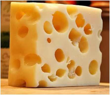
Figure 1 Swiss cheese, image source, http://bgr.com/2015/05/29/why-does-swiss-cheese-have-holes/.
Surprisingly, the reason Swiss cheese has holes has only recently been identified with high certainty, and even now, there is still some debate. According to an article in the Guardian, the latest experiments in Switzerland have identified the root cause as small particles of hay dropping into the milk bucket and getting dispersed in the cheese. As it ferments, bacterial decomposition of the hay makes CO2 which blows bubbles in the solidifying cheese.
The size and density of holes in Swiss cheese over the last 15 years has been decreasing as modern and more sanitary methods have been implemented which keep more hay particles out of the milk.
Regardless of the mechanism, holey Swiss cheese offers a popular metaphor for describing planes with a high density of clearance holes, usually under a BGA escape. Figure 2 shows an example of the worst case clearance hole field in a board, 4 inches x 4 inches. There are about 900 holes in this example.
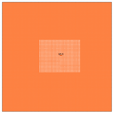
Figure 2 . A holey board with 900 clearance holes, each 35 mils in diameter and on a 50 mil grid, passing through the power and ground planes of the board.
The concern of many designers is the impact on the inductance in the power and ground planes due to all those holes. Since the gaps between them is narrow, won’t they constrict the current, dramatically increasing the series resistance and the loop inductance of the planes?
Many app notes suggest the inductance getting through the field of holes to the center pins is so high, it’s not worth using thin dielectric in the cavity, since the Swiss cheese holes completely swamp any low inductance advantage. These same app notes often suggest that placing decoupling capacitors on the top surface and forcing their current through this hole-field is so ineffective, capacitors should only be placed under the BGA.
Is this really true? While a simple rule of thumb suggests the problem may not be as dramatic as we are lead to believe in these app notes, a quick way to settle this argument is by building a virtual prototype and comparing the impedance profile of the cavity as seen from the center of the cavity.
Electrical Properties of a Cavity as Seen by the BGA Central Pins
We call the structure created by adjacent power and ground planes a cavity. The most important electrical property of a cavity is the impedance between the top and bottom planes, as seen at one port. This topic is extensively covered in the new book I wrote with my buddy Larry Smith, now available from Prentice Hall, Principles of Power Integrity for PDN Design- Simplified (see a preview and chapter 1 here.)
At low frequency, we expect the impedance of a cavity, as viewed from a point in the center of the cavity, to look like a capacitor. The cavity is, after all, just a parallel plate capacitor. All of my students are very experienced in applying the principle of rule #9: never do a simulation or measurement without anticipating what you expect to see.
For this case of a 4 inch x 4 inch cavity, with a 1 mil thick dielectric and a Dk of 4.3, the capacitance is estimated by

I used a value of 1 mil as the thickness so it is easy to see how the capacitance, and inductance, scales to any other thickness. The C increases inversely with h and the L increases linearly with h.
As frequency increases, the spreading inductance from the center of the probing point to the edge of the cavity, as the current flows outward between the top and bottom planes, will begin to increase the impedance. The impedance will continue to increase until the cavity modal resonances affect the impedance.
The spreading inductance should be on the order of 1 square of sheet inductance, which is roughly 32 pH/mil x h = 32 pH.
We can extract a value of the cavity capacitance and the spreading inductance by fitting the impedance profile to a simple RLC series circuit. Figure 3 shows the simulated impedance profile from the central-point of the cavity simulated with Mentor Graphics HyperLynx PI. The circles are the EM simulation. The solid line is the simulated RLC circuit model using a value of C = 15.6 nF and L = 35.4 pH.
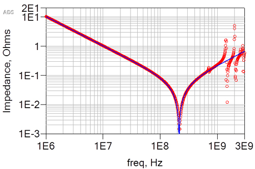
Figure 3. Impedance profile from the EM simulation using Mentor Graphics HyperLynx Pi and an RLC circuit model, plotted with Keysight’s ADS as the solid line.
The match is pretty good, suggesting that the cavity looks like an RLC model at least up to frequencies on the order of 1 GHz, for this cavity. And, our simple estimates of the C and L are pretty good estimates.
Holey Planes, Batman
If we now add the 900 holes to this cavity and simulate the impedance profile with the EM simulator, we would expect the capacitance to not change, as the amount of surface area is not reduced much, but the spreading inductance should increase a little bit.
The fraction of surface area removed by the holes is 35^2/50^2 = 50%. We would expect the sheet inductance to increase by about 50% when we add the holes. Figure 4 shows the simulated impedance of the cavity with holes, compared to without and the new RLC circuit model.
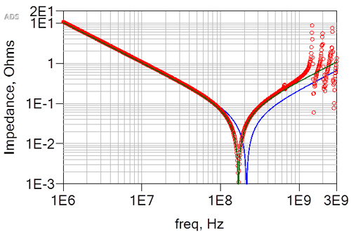
Figure 4. EM simulation of the impedance of the cavity with the holes, as red circles, with the new RLC model in green. The blue line is the RLC model of the solid plane.
The RLC parameters were C= 15.6 nF and L= 53.2 pH. We estimated the increase in spreading inductance should be about 50% with the holes. In fact, we simulated an increase of almost exactly 50% increase.
Holes in the power and ground planes absolutely increase the spreading inductance in the cavity. It’s just that the increase is only 50%. If the capacitor mounting inductance is higher than the spreading inductance, the impact of the holes may not even be seen.
Holey planes are a fact of life when there are a high density of through hole vias under the BGA. The clearance holes will increase the spreading inductance by about 50%. If you care about spreading inductance you should be using as thin a dielectric as you can afford. Given the mounting inductance of the capacitors, compared with the spreading inductance, will tell you immediately if the cavity, even with holes, is still transparent, instead of taking the word of an app note which may just be hype.
The far bigger problem to worry about in a holey cavity is the inadvertent possibility that the clearance holes over lap and create large, contagious gaps in the cavity. These gaps have the potential of generating ground bounce switching noise, a far bigger problem than a 50% increase in spreading inductance.
For more information about spreading inductance and the impedance of cavities, check out Larry and my new book, Principles of Power Integrity for PDN Design-Simplified.