A micromodule device resembles a surface mount IC; however, they include all the necessary support components that would normally be used to construct a power conversion circuit. This includes a DC/DC controller, MOSFET dice, magnetics, capacitors and resistors and so on, all mounted on a thermally efficient laminate substrate. They are then encapsulated using a plastic mold cap. The result was a complete power supply that can be simply adhered to a printed circuit board.
This product family developed at ADI/Linear Tech dramatically reduces risk, time and effort to successfully design high performance, high power density solutions. It is as if we have taken all our power supply expertise and know-how within the company and put it into an IC like form factor. So, for those of you who have had time constraints for designing power conversion circuits where mass production is only weeks away - and you have had to spend many late nights debugging your supply late into the early morning – those times will be a thing of the past - if you use a micromodule regulator instead of a “roll your own” discrete solution.
Taking a closer look at the internal construction of a typical micromodule product, you will notice that the package options are a Land Grid Array or Ball Grid Array (BGA). The internal components used to form the internal switch-mode power conversion circuit can be in die form, while others are finished packaged products. Nevertheless, these components are all mounted onto a Bizmalaleide Triazine (commonly known as BT) laminate substrate which has excellent electrical and thermal properties. Moreover, a micromodule product is not just about integration, they provide other properties and performance characteristics over competing alternatives.
Power Design expertise is declining on a global basis, there are simply not enough power supply design resources to develop every single power supply at most customer’s sites. It is reported by the trade press, that the average age of a degreed engineer is 57 years – and this is a global statistic, with China having the youngest average. Regardless, the clear majority are facing retirement in less than a decade.
The top 3 concerns of these engineers are:
- Insufficient people to get the job done.
- Finding the optimal components for their design.
- Time to market pressures.
Because of these trends, we wanted to deliver a complete power supply that is ready to use off-the-shelf and with all the performance criteria required for the end application. At the same time, PCB area is at a premium since everyone is trying to pack even more functionality and capability into a smaller space. If this is not bad enough already, the thermal design constraints are becoming more complex as designers try to pack more capability into an ever-smaller space while delivering more power in an environment that has limited airflow for cooling purposes. Finally, time-to-market pressures are intense - as the power supply is one of the last items to be designed in a system and mass production starts can be just weeks away.
It is generally accepted that PCB area is at a premium in most designs – you probably know this from your own experience. Take any Datacom or Telecommunications board for example, it is laden with many Digital processors, ASICs and memory. All these need to be powered on the board while voltage levels vary from just north of 5 V to as low as 0.6 V, after an intermediate system bus voltage which varies from 12 to 48 V. At the same time, system designers are continually being asked to pack more functionality into these ever shrinking from factors – which are probably mutually exclusive!
Design problems that needed to be solved
Thermal design constraints are becoming more severe. As more and more functionality is packed onto the PCB, the overall power levels needed to power them on the board are increasing. Meanwhile, cooling is at a premium due to heat sinking space constraints and limited air flow volume. This is a headache for the designer since he has a maximum internal ambient temperature constraint for his system that he cannot violate with compromising performance and long-term reliability.
Time-to-market pressures have increased dramatically in recent years due to both competitive pressures and the need for faster revenue streams. So, the power supply designer is under-the-gun for getting his power conversion circuits designed and functional in weeks…if not days. Micromodule products provide a “simple & done” proven power conversion solution. Of course, these products need to have rigorous quality and long-term reliability to ensure long operational life once they have been deployed in an end system. Accordingly, ADI has engaged in rigorous quality and reliability testing to ensure long term deployments in harsh environments.
Below is a summary of the testing and data we have accumulated since the introduction of our first product, the LTM4600 back in October of 2005. This includes:
- Over 22 million power cycles
- Over 5 million device hours of hot temperature operational life
- Over 2 million hours mounted temp cycles to ensure that these modules can operate 24/7, 365 days per year for a decade without having any intermittent contact issues from the package leads to the PCB
- Over 25 million temp cycles from -65ºC to 150ºC.
- Over 16 million thermal shock cycles from -65ºC to 150ºC. And remember, this is liquid-to-liquid on a finished power supply!
The end outcome is a FIT rate of < 0.4. To put this in perspective, this equates to 0.4 device failures in every billion device hours of operation. And this is on a complete power supply. To put this in context, many of the competitors’ integrated circuit (single silicon in a package) have higher FIT rates.
Packaging Evolution
Let’s take a closer look at the micromodule packaging options. When we first introduced the LTM4600 way back in October of 2005, we used a Land Grid Array (LGA) package option. The thinking at the time was the since a lot of the VLSI Digital ICs had a similar LGA form factors, it would be easy for the user to use our micromodule products. Well, while this was true some of the time, it was not true all of the time.
Accordingly, it was decided that having a Ball Grid Array (BGA) package option would be an innovative idea too. This turned out to be fortuitous for two reasons. First, it was easier for users who were not used to high volume production of the LGA’s. And, secondly, it was easier to put solder balls on the round pin pads. Moreover, it allows for both leaded and lead-free solder balls. And since many micromodule users are in the Aerospace and Military market segments – they were very happy about this.
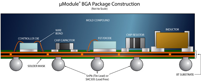
Figure 1. Micromodule Regulator BGA Package Cross-section.
Accordingly, the first part we introduced in this product category was named the LTM4600; a 4.5 to 20 V Input/0.6 to 5.5 V Output and up to 10 A of continuous output current. It was in a 15 x 15 x 2.82 mm surface mount LGA package. Its “killer” application was 12 Vin to 3.3 Vout at 10 A with 90% efficiency. Remember, this was October 2005, so, this level of performance was ground breaking stuff.
Nevertheless, one of our key metrics was to improve the micromodule regulators thermal performance so that we could increase its output current density while remaining in same the 15 x 15 mm footprint. Since there was clearly a significant thermal issue we needed to address getting the heat out of the package. To facilitate this goal, our designers had decided to use a BT laminate substrate because it had excellent thermal properties and facilitated taking heat though the bottom of the micromodule package and into the PCB where it could be dissipated. While this was acceptable in the mid-2000s; by the time another 5 years went by, our customer-base informed us that they could no longer dissipate most of the heat through their PCB. Instead, it needed to be able to pull heat out of the top of the package and dissipate it into the air! Therefore, we designed a special heat sink that was encapsulated inside the package and connected to the top of the internal MOSFETs and inductors. This heat sink was exposed on the top side of the micromodule regulator. Now the user could add their own heat sink on top of the micromodule device to improve pulling heat out of it. Or, if they had 200 LFM or airflow, also facilitate better thermal performance. eat sink to further improve thermal dissipation qualities.
Finally, it should be mentioned why we introduced our Ultrathin micromodule devices. We realized that in many cases our customers would only utilize the underside of their PCBs with discrete component due to space limitations. It turns out that for many rack mounted systems there was a 2.2 mm of height restriction for mounting components on the underside of a PCB. Therefore, we developed micromodule regulators with 1.8 & 1.9 mm maximum height so that they would easily fit and help with space and density issues.
Now, with this background, it is easy to comprehend what is going on with a micromodules’ thermal performance. This can be thought of as an evolutionary pathway that has allowed for a continuous improve our micromodule thermal performance from inception through to our current offerings: a decade plus journey.

Figure 2. Thermal imaging of a micromodule regulator construction and heat dissipation
Figure 2 shows three thermal imaging photographs, representing several types of micromodules with varying types of construction with the goal of increasing the devices ability to pull heat out of the top of the micromodule into free air; where it can facilitate additional cooling from air flow within the system or could also have an additional heat sink that is shared with the VLSI Digital ICs that are usually present. The blue color shows low temperature (minimal power dissipation) and colors orange through red are elevated temperatures (high power dissipation). Of course, this is what we want to occur when we want the heat generated by the power conversion process to pulled out into free air and not into the PCB.
While we have been improving thermal performance characteristics of this product offering, we have simultaneously continued increase micromodule regulators’ power density by putting them into ever shrinking form factors. In Figure 3 shows the LTM4627, a 20 V input device and can deliver 15 A output current as low at 0.6V with an efficiency in the nominal 90% range depending on the specific Vin and Vout conditions. Next to this is the “soon-to-be” released LTM4638, that is also a 20 V input device and can deliver a 15 A output as low as 0.6 V with nominal 86% efficiency. However, volumetrically, the LTM4638 is 5.6 times less than the LTM4627. See Figure 3 for a size comparison.
The point being that there is only a small delta in conversion efficiency between these two parts under the same operating conditions, but the footprint and space required for its implementation are orders of magnitude less. And all this improvement has all been attained in less than 4 years.

Figure 3. LTM4627 (15 x 15 x 4.92 mm) versus its new, smaller equivalent, the LTM4638 (6.25 x 6.25 x 5.02 mm)
Sojourn to a single 100 A micromodule device
For a long time, our existing users of high power micromodule packages kept asking us for smaller, more efficient and higher current density devices – even though this feature set might be considered mutually exclusive. Nevertheless, our design team took this request to heart and began to figure out a way to get us there.
From a Historic perspective, back in the 2013 to 2016 timeframe we had micromodule regulators in the 15 x 15 mm foot print which are capable of delivering output currents in the 26 to 50 A per device range. It should also be noted that a key matrix measurement for our high power micromodule devices is that they should be able to deliver full rated output current from a 12 V input to a 1 V output with 90% conversion efficiency. The reasoning being that dealing with 10% power lost as heat is usually thermally acceptable within most applications. By late 2016, our 40 A+ micromodule regulators we had efficiencies in the 88% to 89% range – which is very close to this goal.
The progression to get to a 100 A single micromodule regulator required us to use multiple devices, as shown below:
Thus in 2010, having 12 x LTM4601’s in a Polyphase® parallel configuration allowed us to deliver 100 A output from a 12 to 1 V output.
In 2012, only 4 x LTM4620’s in a Polyphase parallel configuration allowed us to deliver 100 A output from a 12 to 1 V output.
In 2014, only 3 x LTM4630’s in a Polyphase parallel configuration allowed us to deliver 100 A output from a 12 to 1 V output.
In 2016, only 2 x LTM4650’s in a Polyphase parallel configuration allowed us to deliver 100 A output from a 12 to 1 V output. And, we have +/-1% total DC error over line, load and temperature.
Finally, in November 2018, we introduced the LTM4700 – a dual 50 A or Single 100 A output micromodule regulator. See Figure 4 for a photo of the actual device.

Figure 4. The LTM4700 capable of delivering up to 100A output current in a single package
Figure 5 shows a thermal image of the LTM4700 during normal operation. The operation conditions are 12 to 1 V delivering 100 A of current with high conversion efficiency and only 200LFM of airflow. As a result, its best in class energy efficient performance makes it an excellent choice to reduce data center infrastructure cooling requirements.
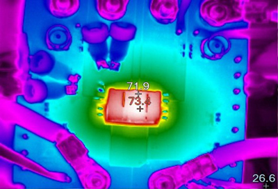
Figure 5. LTM4700 100A mModule (89.6% efficiency)
Taking a closer look at some of the LTM4700’s key specifications, we have:
- It is a single 100 A output capable micromodule. Or, it can be used as two 50 A outputs.
- It is very close to 90% conversion efficiency when stepping down from 12 to 1 V at 100 A with only 200 LFM air flow. And has +/- 0.5% maximum DC error over temperature.
- Its x, y, z footprint is 15 x 22 x 7.82 mm.
- The LTM4700 is formally released and samples are available for evaluation purposes.
In addition to having a dual 50 A, or single 100 A output, the LTM4700 also incorporates a PMBus I2C interface or Power System Management. We call it PSM for short. This enables many different capabilities, including the following:
A) Configure voltages, define complex on/off sequencing arrangements, define fault conditions such as OV and UV limits and set important power supply parameters such as switching frequency, current limit, etc. over a digital communication bus.
B) Over the same communication bus, you can Readback important operating parameters such as input voltage and output voltage, input and output current, input and output power, internal and external temperature and in some of our products measure energy consumed.
C) Users can implement very precise closed-loop margin testing of their designs as well as trim power supply voltages to very precise levels
D) A system benefit of using our PSM devices is higher reliability and quality
E) Our built-in servo loops will maintain higher power supply accuracy over the life of the product improving reliability
F) The readback features of our PSM devices can be used to improve test coverage at In-Circuit-Test and screen out possible defective devices before they get into the field.
G) During the life of the customers product our PSM devices continue to monitor important parameters. Trends in voltage, current and temperature can be used to profile the power system. Once a good system signature can be found, a flawed system or one that is about to fail can be identified.
Conclusion
We introduced our first micromodule regulator back in October of 2005, the LTM4600. It came in a 15 x 15 x 2.8 mm land grid array package and could deliver 10 A of output current from a 12 V input to a 1.2 V output with 89% efficiency. Fast forward 13 years and have the LTM4700 which can deliver 100 A from 12 to 1 V with 89.6% efficiency (and 200LFM air flow). But that’s not all, we haven’t stopped here, our designers are already working on other modules that can enable even more performance and capabilities. So, remember to keep up-to-date on our products for what is ahead of what’s possible.