
B. Layout consideration
The DAC having a resolution of 12 bits plus its 4:1 MUX, it means that there are 48 bits to interface. Moreover, at this speed, differential signaling is necessary and a total of 96 PCB traces are layout between FPGA and DAC through multiple layers. Adding to that, in order to limit the package skew which is different for each bit, every group of 12 bits (24 traces with differential signaling) is layout to the same bank of the FPGA. This adds a slight complexity to the layout but is required to reach these high-speed with a parallel interface.
As mentioned in section II, the traces lengths of the data lanes also need to be matched to limit the bit to bit skew. And this is complicated to achieve with 96 traces. In Figure 3, a photo of the board is shown. The meanders are generally the solution used to match the traces length (same principle as an interface to a DDR3 memory for example).

Figure 3: Electrical board
Note: The distance between the FPGA and the DAC is due to one of the board requirement. This board has been used to characterize the DAC and as such it was necessary to be able to control the DAC temperature without affecting the surrounding component. In a real application, even though the requirement to match the trace length can impact the distance FPGA-DAC it would still be much closer.
This shows the complexity that can be brought to the layout phase when working with parallel interface with huge bandwidth (in this case 72 Gbps are transmitted between FPGA and DAC). Nonetheless the latency achieved is impressive as there is only 3 clock cycles – or 500ps at 6GSps - between the DAC input and analog output.
C. FPGA consideration
For the FPGA, a lot of consideration is necessary before choosing it. When working with high-speed parallel interface, it is necessary to spend time to look at the timing uncertainties and make sure that the FPGA and the right speed grade are targeted.
The SERDES component is used to output the data from the FPGA at the required speed of 1.5Gbps. It is a serializer (same principle as for a serial interface but at lower speed) which takes in this example chunks of 8 bits at 187.5MHz and output them at 1.5Gbps. This also allows isolating the FPGA fabric from the fast transmission and being able to do some processing within the FPGA at respectable clock speed. Depending on the processing being done a serialization by a factor of 4 instead of 8 could have been possible but would have required more care to respect the timings within the FPGA. However this would be a way of improving latency performance. The SERDES component is in four parts each one linked to one of the port of the DAC. As such, the reset signal needs to be synchronously sent to all SERDES block to ensure that the data are aligned between the different ports of the DAC.
Another feature can be added to help correct for bit to bit skew which allow adding independent digital delay on each of the bit path. Both static and dynamic solution exists depending on the FPGA. The benefit of this feature is that it can help open the eye even more and thus allows for faster transmission speed. However this can be hard to implement as to be effective it should be tuned independently for each board/system and thus is not viable for an industrial scale application without automation.
Example of ESIstream serial interface between ADC and FPGA
A. System overview
This example of a serial interface is based on the evaluation system of the EV12AD500A. It is composed of the EV12AD500A, a 12 bits dual-channel 1.5GSps ADC [3] and the Virtex 7 from Xilinx [4]. The Figure 4 below shows a block diagram of the system.

Figure 4: Block diagram of the ADC-FPGA interface
The serial link in this example is running at 6Gbps and there are 8 links used to transmit 48Gbps. Within these data transmitted 13.5% are overhead due to the protocol. Comparing to the parallel interface, and extrapolating if they both transmitted the same amount of useful data, the gain in the number of lanes to layout is 75%.
B. Serial interface protocol
It has been mentioned earlier that without protocol a serial interface would see huge BER loss. This is due in part to the CDR and in part to the AC coupling. The CDR objective is to recover the clock form the data stream. In order to do that, it needs to see edges in the data otherwise it can’t identify the clock. Hence, long series of successive ‘1’ or ‘0’ need to be avoided for a serial interface. The interface between TX and RX has to be AC coupled; at these high-speed a small difference in the common-mode added to all the other effect could contribute to a degradation of the BER. This AC coupling means that if the data stream transmitted is not DC balanced (as many ‘1’ and ‘0’ transmitted), the AC coupling capacitor will get loaded and corrupt the data seen by the reception stage. The protocol’s objective is to prevent both long series of ‘0’ or ‘1’ and a non-DC balance transmission from happening.
The ESIstream protocol used in this example is one of the available serial interface protocols like JESD204B, Interlaken and many others. It brings interesting benefits such has optimized efficiency and latency, simplicity and ease of design. Documentation and example design on this protocol can be found on its dedicated website [5].
C. Design consideration
As mentioned earlier, when working with serial interface, the encoding/decoding process requires digital resources to be implemented. Generally speaking the objective is to reduce this impact as much as possible so that the resources can be saved for the intended processing of the application. In this objective, the FPGA design needs to be oriented toward resource optimization while still being able to transmit the data and detect whenever an issue occur. And the ratio between optimization and issue detection is very dependent upon the transmission data rate. A transmission at 6Gbps does not require the same detection and correction process than a transmission at 32Gbps to reach a similar BER.
Looking in more detail at the FPGA design for the interface in case of the serial interface, Figure 5 below shows the architecture of the reception stage in the Virtex 7.
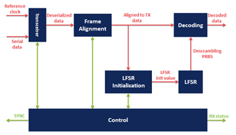
Figure 5: FPGA RX architecture
To understand this architecture, some information on the ESIstream protocol is required. This protocol is using a 2 stages encoding and 2 overhead bits process. One is a scrambling process, the other one a disparity process. The scrambling process is using a Linear Feedback Shift Register (LFSR) to generate the scrambling/de-scrambling pseudo-random sequence. A synchronization sequence is used to initialize the link and align the TX encoding and RX decoding through the frame alignment component. Finally the decoding takes place where the descrambling is realized and the disparity processed. For more information you can refer to the ESIstream website [5].
In terms of resources and latency required by this specific implementation they can be found in Figure 6 below.

Figure 6: Resource and latency figure for serial interface
The values concern the FPGA implementation used in this example for the RX. The TX values correspond to an FPGA equivalent to the ADC. The difference is that the ADC process allows it to work faster than the FPGA and thus the ADC latency is 10ns for the TX compared to the 30ns reached using an FPGA.
It can be noted that in terms of latency; with serial interface it extend to a total of 60ns (using the ADC value for the TX). Compared to the parallel interface presented earlier there is two orders of magnitude loss that would be incompatible with some application.
Conclusion
This paper has presented the difference between parallel and serial interface and which key factors to consider before choosing; accompanied by 2 examples to introduce a quantitative comparison. Even though serial interface have become the ubiquitous solution in the past years, a few application still have requirement forcing them to use the parallel interface. This is bound to keep evolving and already today modulated serial interface [6] starts to appear to reach the next step in high-speed data transmission bringing more problematic to solve.
References
[1] e2v EV12DS460 product page:
http://www.e2v.com/products/semiconductors/dac/ev12ds460/
[2] Altera Arria V product page:
https://www.altera.com/products/fpga/arria-series/arria-v/overview.html
[3] e2v EV12AD500 product page:
http://www.e2v.com/products/semiconductors/adc/ev12ad500/
[4] Xilinx Virtex 7 prduct page:
https://www.xilinx.com/products/silicon-devices/fpga/virtex-7.html
[5] ESIstream protocol website:
www.ESIstream.com
[6] PAM-4 Design Challenges and the Implications on Test, Keysight Technologies