
In my consulting work, most of the low-frequency (150 kHz to a few MHz) conducted emissions in power converter applications are caused by differential mode (DM) radio frequency (RF) noises. Root causes of such noises include poor DC link design, lack of snubber circuit for the switches and inefficient DM filtering. Recently, however, significantly high levels of common mode (CM) noise were seen at the low-frequency end in a few applications.
Challenges associated with low-frequency CM noise include:
- The impedance of ferrite cores is very low at such frequencies, making them ineffective.
- Y-Class capacitors are effective, but the leakage current requirement limits the value of the capacitors.
- Shielding can work; the thin line between a pass and a fail often depends on where to terminate the shield.
These challenges mean that a retrofit approach cannot be easily achieved, and a redesign is often considered costly from the manufacturers’ point of view.
This article presents a couple of case studies where troubleshooting tools such as RF current probes and resistive probes proved effective in troubleshooting low-frequency conducted emissions. The root causes of low-frequency CM noise are also explained and recommendations for fixing such issues are proposed. The “CM noise mapping” and converting CM noise to CM voltage in LISN are novel techniques which could accelerate the EMI troubleshooting process.
Case Study 1: A Charging Station for Electric Vehicle Applications
An electric vehicle (EV) charging station failed the conducted and radiated emission tests in the EMC test chamber. In this case, the device under test (DUT) is a 60-kW unit powered by a three-phase power supply. The high cost of renting the test facility and the transportation of a large installation make EMC troubleshooting in the test chamber costly.
Testing and troubleshooting the DUT at the factory site proved to be a cost-effective solution for the manufacturer. A three-phase LISN rated for 75Amp is hard to rent (in the UK) and would require a large isolation transformer to prevent it from tripping the circuit breaker at the customer’s factory site. Therefore, a pair of matched RF current probes were used as the primary troubleshooting tool for conducted emissions. The concept of using a pair of matched current probes was first introduced in [1]; in our case study, the matched pair ensures simultaneous measurement of the RF current in the subsystems of the DUT.
RF current monitoring probes are widely used for measuring and troubleshooting EM emissions on cables. In [1], Smith demonstrated ways of extending the usage of current probes in EMI troubleshooting, which includes extending its low-frequency response, using a pair of matched probes for advanced troubleshooting, and measuring a conductive voltage drop on a cable. Wyatt discussed the theory and application of RF current probes in [2], including detailed instructions for making and characterizing a homemade probe.
Figure 1 illustrates a pair of matched current probes used in two locations of the DUT. The DUT was powered directly from the mains (No LISN was used). One probe was clamped around L1,2, 3 and the neutral wires at the mains entry point of the unit (before the filter) to measure the CM current, while the other probe was located just after the filter. Figure 1 also shows the measured CM current (in dBμA) on the three-phase mains cable. The noise profile is similar to the test chamber's LISN measurement (Conducted emission on L3 is shown in Figure 1). The following equations were used to obtain the RF current reading in dBμA.
I(μA) = Vprobe(μV) / ZT(Ω)
I(dBμA) = Vprobe(dBμV) - ZT(dBΩ)
Where Vprobe is the current probe reading from the spectrum analyzer. ZT is the probe's transfer impedance (frequency dependent), which one can find in the manufacturers’ datasheet.
There were two resonance peaks in the result, with one resonance sitting at 1.5 MHz and the other close to 6.8 MHz. These noises were caused by the off-the-shelf AC/DC converters used in the DUT and can be suppressed easily by placing ferrites at the AC input wires of the converters. The low-frequency noise in the 150 kHz to 700 kHz range was difficult to eliminate by the ferrite cores as the impedance of ferrites at this low-frequency range is low.
|
Figure 1. Current probe measurement shows a similar profile as the LISN measurement |
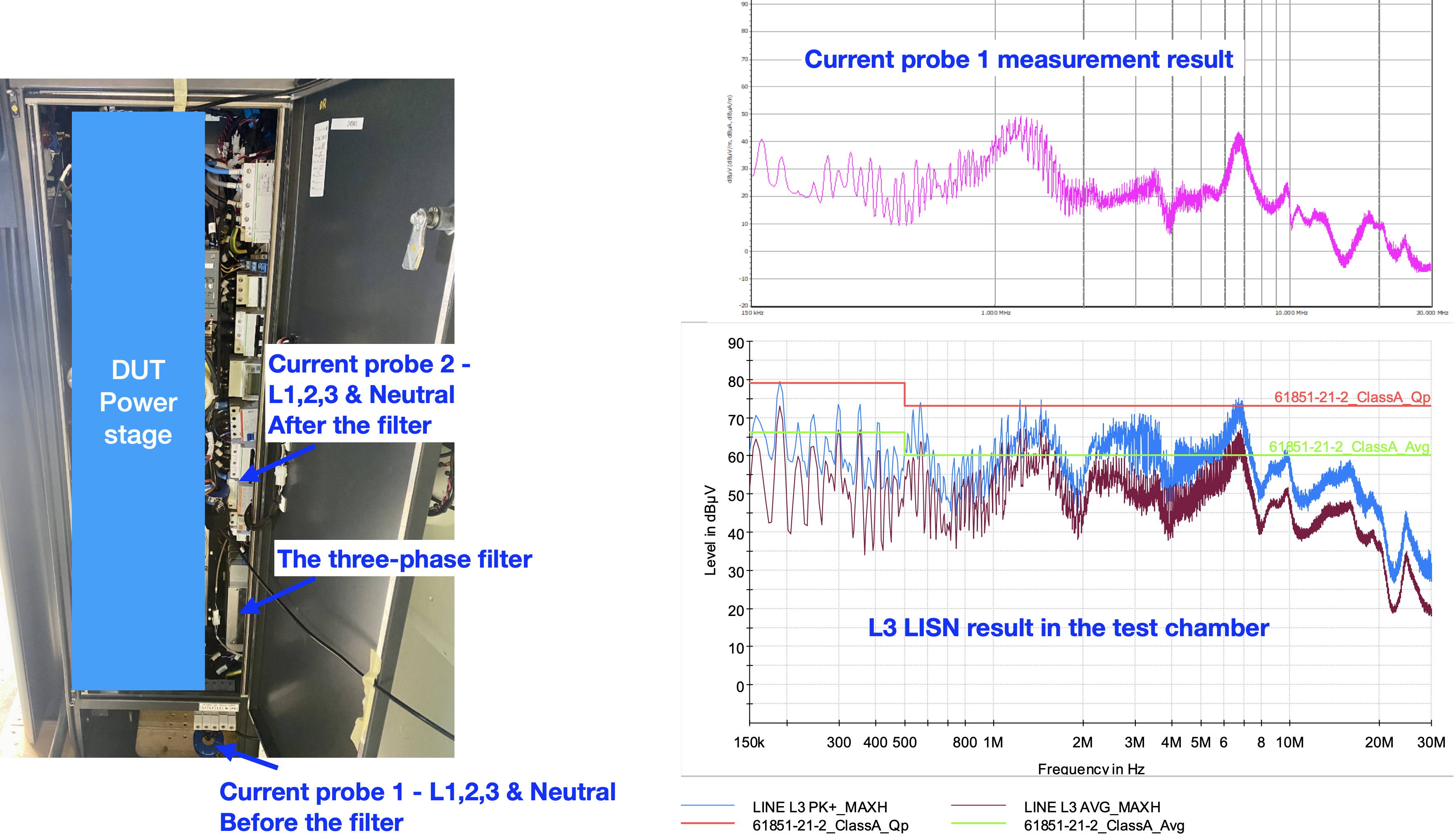
Figure 2 demonstrates the comparison results between probes 1 and 2 in the frequency range from 150 kHz to 10 MHz. As can be seen, the three-phase filter suppressed the CM noise by a certain degree (more than 30 dB in most of the frequency range) but was still shy of a few dB to pass the test. The LISN result in Figure 1 suggests an extra 6 dB reduction was needed to ensure a pass in the conducted emission test.
|
Figure 2. Comparison CM current results of a pair of current probes; Probe 1, CM current before the filter; Probe 2, CM current after the filter. |

CM Noise in the Low-Frequency Range
The high level of CM noise in the DUT contributed to the conducted emission failure. A clear understanding of the noise propagation path is needed to solve the noise issues.
Whether the noise is DM or CM depends strongly on the coupling path to earth (in this case, it is the true earthing point as the RF reference). In a single-phase power system, products whose live and neutral wires are double insulated do not require earth wire connection, so the capacitance to earth is extremely low. Therefore, the impedance to the earth is mostly dominated by the impedance of the artificial hand.
Industrial equipment (often powered by a three-phase supply) is usually earthed and has a sizable earthed heatsink with the power switching devices bolted to it, this forms a high capacitance from the noisy node of the switching converter to earth as shown in Figure 3. When the switches are turned on and off at a fast speed, a large amount of CM noise is introduced because of the Cdi/dt. A 10 nF capacitance from the transistors to earth is not uncommon, at 200 kHz, the impedance is only 80 Ω.
|
Figure 3. Power switching devices are bolted to the heatsink which is often earthed |

Understanding the CM noise propagation path provides solutions to the issue. One way of reducing the noise is to reduce the capacitance from the noisy node to the earth. This can be done by floating the heatsink, though this approach often requires sufficient air-cooling in the system.
Sometimes, a shield between the transistor and the heatsink can work well, which worsens the thermal conduction path. This, again, demonstrates the trade-off that a design engineer often faces between efficiency and EMC. Other times, a choke/ferrite in the earth line helps, but this can make radiated noise worse.
Troubleshooting and Problem Fixing
Once the CM noises were measured before and after the filter, the same current probes were then used in the critical common mode propagation paths in the DUT including the AC cable of the rectifiers, the DC link bus wires, control cables, ethernet cable links, and so on. This is a technique we call “CM noise mapping.” This exercise identified the DC link as a “hot area” where a significantly high level of CM noise was observed.
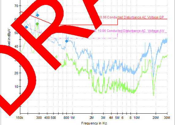
Two capacitors from the DC bus wires to the heatsink were placed to reduce the noise, the temporary fix (for troubleshooting only, not the final implementation) was shown in Figure 4, where the capacitance value of each capacitor was 330nF, it can be seen that the noise measured behind the filter was reduced, especially at the frequency points of interest (180 kHz, 300 kHz and above). The touch current was also checked to ensure no excessive leakage current was caused by the extra capacitance added to the system. Subsequent tests in the EMC chamber showed a pass for the conducted emission tests when a properly designed capacitor PCB was retrofitted to the system.
|
Figure 4. Adding capacitors between the DC bus wires to the heatsink reduced the CM current measured after the filter |

Case Study 2: An On-Board-Charger for EV Applications
An on-board-charger (OBC) for EV applications failed the conducted emission tests during the vehicle level EMC charging tests. The failure frequency range is between 200 and 300 kHz as shown in Figure 5. Note that the neutral wire result is shown in this case, but the profiles of other wires are almost the same as the neutral, suggesting the CM noise might be the dominant noise. It should be noted here that the OBC had passed the component level test with a good margin, the vehicle level failure indicates that the wiring and harnessing of the OBC might have contributed to the noise when it was mounted on the vehicle.
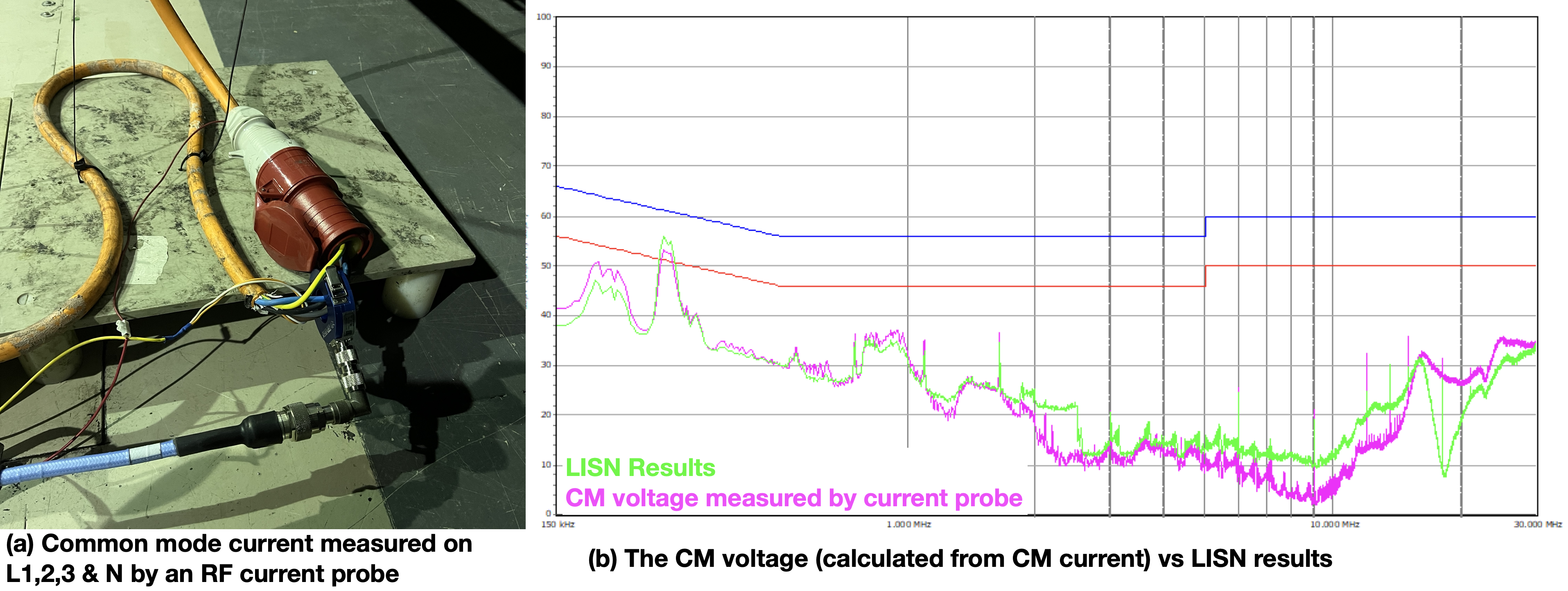
In this case, the investigation was performed in a vehicle test chamber where a three-phase LISN was available during the fault-finding stage. A current probe was clamped around L1, 2, 3, and neutral wires to measure the CM current. Since a three-phase LISN was used in this test, one can calculate the LISN common mode voltage from the CM current [3]; this is explained in detail.
|
Figure 5. Conducted emission of the OBC (neutral) |
|
Figure 6. The CM voltage relationship to CM current |

Figure 6 illustrates the CM noise voltages VCM, derived from the total noise voltage of each power line, V1, V2, V3, and VN. The CM voltage component is a quarter of the vector sum of V1, V2, V3, and VN. When a current probe is placed around L1,2,3 and the Neutral line, the total amount of CM current measured is 4×ICM, we can then derive the CM noise voltage as
VCM = 50 × ICM = 50 × Iprobe/4 = 12.5 × Iprobe
VCM(dBμV) = 22 + Iprobe (dBμA)
Where VCM is the CM voltage measured by the LISN and Iprobe is the RF current probe reading in dBμA.
When factoring the 22 dB into the current measurement result, the CM voltage can be obtained; this result was then compared with the LISN measurement, as shown in Figure 7. The conducted noise is predominantly CM in this case.
|
Figure 7. (a) A current probe is clamped around L1,2,3 & N; (b) comparison between the CM voltage and the LISN result |
The fact that the conducted emission noise is common mode means that the earth wire of the OBC will carry a large amount of the CM noise. The earth wire of the OBC had a splice in this case, where one was connected to the EV charger, and the other was connected to the vehicle chassis. It was the chassis connection that caused the failure. To prove this, we measured the surface current on the chassis bracket where the earth wire was connected using a homemade resistive probe. The resistive probe was first introduced in [4]; the probe tip is shown in Figure 8. It was shown in Figure 8 that when the OBC was operational, the low-frequency noise on the chassis was significantly high.
When we disconnected the earth wire from the chassis bracket, the conducted emission was reduced. Note that the earth wire was still earthed via the charging connection, so the safety aspect was not compromised.
|
Figure 8. Using a homemade resistive probe to measure the surface current on the chassis |

Conclusion
As power electronics devices are bolted to the heatsink in a power converter, a significantly high level of CM noise can be introduced because of the parasitic capacitance between the switch node and the heatsink. Understanding the noise path is essential to solve the emissions. This article presents a few useful troubleshooting techniques to accelerate the troubleshooting process.
References
[1] |
D. Smith, “Current Probes, More Useful Than You Think.” |
[2] |
K. Wyatt, “The HF Current Probe: Theory and Application.” Interference Technology, 2012. |
[3] |
M. Zhang, “Separate Common-mode and Differential-mode Signals.” |
[4] |
D. Smith, “A Resistive Current Probe.” |