
The process of extending the digital throughput of a software defined radio (SDR) to 40 Gbps and 100 Gbps is complicated and entails addressing various challenges, including difficulties in maintaining signal integrity, implementing 100G Ethernet IP cores in a field programmable gate array (FPGA), and adapting the host computer to sustain high performance and high data rates.
This article explores how signals are captured and converted from analog-to-digital or digital-to-analog in a lossless fashion. It discusses various considerations including selection of a suitable substrate for high frequency applications and achieving low impedance. The article also discusses how high data throughput Ethernet is implemented on FPGAs to enable packetization of IQ sample data. Lastly, the article explores how host or server systems with high data throughput capability are used to handle the huge amounts of data exchanged between the FPGA of a SDR and network interface cards (NICs) of a host system.
mmWaves Bands
Millimeter waves (mmWaves) have wavelengths that range between 1 and 10 mm, in the band commonly referred to as extremely high frequency (EHF). Some of the main challenges facing mmWave propagation include high attenuation and high susceptibility to blockage by obstacles. Despite these challenges, this radio band (30 to 300 GHz) is attractive for data transmission applications because it is suitable for applications involving transmission of huge amounts of data, such as gigabit wireless service, since more data can be carried at mmWave frequencies than at lower frequencies.
mmWaves are used in a wide range of applications including astronomy, remote sensing, security screening, satellite imaging, and 5G telecommunications. The plan to employ mmWave technology in 5G networks is probably one of the most promising applications, as studies have shown that 5G networks using these frequencies can deliver ultra-low latency (<1 ms latency) and very wide bandwidths (10-20 Gbps).
The rapid growth in the number of applications with high bandwidths is increasingly making it necessary to process huge volumes of data in the digital domain. Processing and transferring such amounts of data requires ultra-fast multi-gigasample/second (GSPS) analog-to-digital and digital-to-analog converters (ADCs/DACs) and ultra-fast communication links. Examples of applications that require this level of performance include edge computing and spectrum monitoring applications. These kinds of applications demand FPGAs with 100G Ethernet for transferring data.
SDRs for mmWave applications
A SDR system is a transceiver that utilizes flexible software-based components and is capable of performing complex signal processing capabilities. A typical SDR system has three main parts: a radio frontend (RFE) that handles analog signals, a digital backend that operates on digitized signals, and an interface that handles mixed signals. The RFE offers multiple independent transmit and receive channels, with each supporting a wide frequency tuning range, typically tens of gigahertz.
The digital backend features an FPGA that allows high-speed transfer of data between the SDR and host system. The highest-bandwidth SDRs offer high instantaneous bandwidths of up to 3 GHz. The FPGAs used in high performance SDR systems feature various onboard digital signal processing (DSP) capabilities including demodulation, CORDIC mixing, data packetization, upconverting and downconverting, and application-specific functions such as artificial intelligence/machine learning (AI/ML) and security schemes. The mixed signal interface consists of dedicated ADCs and DACs that convert signals from one format to the other. Figure 1 shows a simplified block diagram of a high performance SDR system.
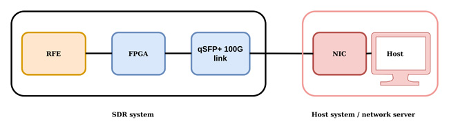
Figure 1. High level overview of a Per Vices Cyan high performance SDR system.
High performance systems are suitable for a broad array of wireless applications. The 3 GSPS ADCs and 4 x 100 Gbps links of the recently upgraded platform enable higher throughput and bandwidth as compared to its predecessor which features 1 GSPS ADCs and 4 x 40 Gbps links. Moreover, the system can be upgraded to support applications utilizing the extremely high frequency band.
FPGA 100G Challenges and Solutions
Various challenges are encountered when implementing FPGA designs for high data throughput SDR. To start with, as the width and speed of the bus increase, it becomes more difficult to meet the timing requirements. This can be seen in the fact that 40G Ethernet uses 128-bit words while 100G Ethernet uses 512-bit words. For instance, when implementing 100G, with a clock center frequency of 390.625 MHz (100G) and at 512 bits/word, the signal is valid after every two blocks (390.625*512 = 200 Gb/s so signal is only valid every other clock cycle since 200/2 = 100 Gb/s). Handling this properly in a FPGA is usually difficult.
Implementing an FPGA-based system that supports data transmission rates of 100G entails addressing a variety of design challenges and requires strict adherence to good design practices. Some of these practices include correct handling of signals and reducing combinatorial paths. This is important since each input signal data needs to be stable before (setup time) and after (hold time) of the rising edge of the clock for the sequential combinatorial logic to be executed in each signal path while respecting this clock, as shown in Figure 2.
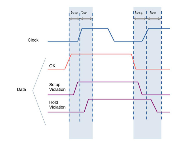
Figure 2. Setup and Hold time of a data signal that must respect the rising edge of a clock.
If the FPGA design has setup or hold time violations, the flip-flop output is not guaranteed to be stable, meaning that it could be zero, it could be one, or somewhere in the middle; a property called metastability. One of the design techniques that is commonly used in reducing combinatorial paths is pipelining. Pipelining basically entails adding flip flops along the path of a circuit to reduce path delay (both combinatorial and routing delays), such that it respects the clock and helps to maximize the throughput of a high-speed system. Of course, pipelining is not without consequence, as it tends to increase latency.
High-Speed PCB design Challenges and Solutions
The performance of a high-speed system is greatly determined by the quality of the PCB used. To prevent degradation of signals, special attention should be given to PCB materials, traces and couplings. In most cases, PCBs for use in high-speed applications have tens of layers and hundreds of traces. For such PCBs, it is critical to consider attenuation, impedance mismatch, and inductive/capacitive crosstalk since they greatly influence the overall performance of a system.
The performance of high frequency applications is also greatly determined by the resistive loss of the traces roughness. At high frequencies, the current flowing in a copper trace is restricted near its surface, a phenomenon referred to as skin effect. The result is that effective resistance increases with a decrease in the cross-sectional area (A) of the material. Since current follows the contours of the surface of the copper, the effective of surface roughness is an increase in the distance over which current must flow (L) and hence the resistance of the copper increases (since R=pL/A, where p is resistivity, L is the length, and A is the cross-sectional area).
Also, at high frequencies, the fiber weave effect becomes problematic. Figure 3 shows fiber weave effect in different materials.
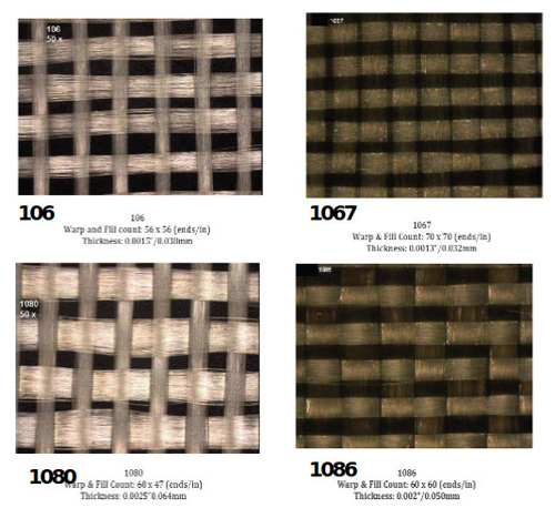
Figure 3. Fiber weave effect in four laminate materials (recreated from this source).
Any fiber weave effect results from the periodic variation in the weave pattern throughout the PCB substrates. Since the fiber weave results in a repeated variation in the dielectric constant of the substrate material, the dielectric constant of the substrate weaves is anisotropic, meaning the dielectric constant seen by a signal running along a trace also depends on the direction the signal travels. Fiber weave effect is more profound in conductor traces with rough surfaces. This can be seen in Figure 4 where each trace has a different characteristic impedance based on the direction it is routed.
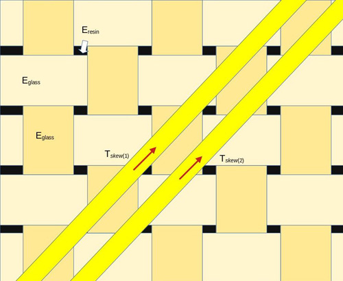
Figure 4. Fiber weave effects on multiple traces routed in directed areas of the substrate material.
When designing a PCB for high-speed applications, it is critical to address each of the challenges discussed here. To begin with, a careful selection of a conductor is required to ensure optimal performance of signals throughout the system. In addition, using differential signaling is one of the strategies used to improve the performance of PCBs for high-speed applications. This technique helps to ensure that the functionality of the data link is maintained even when the attenuation level is high. Secondly, it ensures robust performance even in cases where the quality of the ground connection is not guaranteed. As compared to single-ended paths, differential signaling supports higher data rates.
One way of reducing losses in PCBs is employing low loss laminates in the design. For PCBs for use in high-speed applications, it is essential to use ultra-low loss laminate materials such as Tachyon 100G. Tachyon 100G offers excellent electrical properties and is ideal for data speeds of 100 Gbps and beyond.
Fiber weave effect can also be minimized by employing a variety of strategies in the PCB design. For starters, it is advisable to use uniform glass material such as 3113 or 2116 to ensure that there are minimum variations in impedance. Secondly, it is advisable to use wide traces in your PCB and ensure they are routed at an angle to the fiber warp. Studies have shown that using zig-zag can greatly help to minimize fiber weave effect in PCBs. Furthermore, it is recommended to use materials that have similar resin and fiber dielectric values.
Designing Host Systems for 100 Gbps Ethernet Challenges and Solutions
There are many challenges in designing a host system that can support 100 Gbps Ethernet. On the SDR’s side, the FPGA guarantees synchronous and deterministic performance, and the transfer of data is uniform and monotonic. Data transfer on the host’s side is prone to latency and jitter. Careful consideration is required to ensure that latency and jitter related issues are properly managed to prevent silent dropping of data within the networking buffers or at the NIC.
Writing from memory to disk can be challenging in applications involving many channels and a wide bandwidth. It is critical to ensure that a sufficient write speed is maintained between the two. Transmitting data at high speeds is a challenging task owing to the difficulty involved in maintaining the required buffer level. The task also has stringent latency and jitter performance demands that are difficult to maintain.
Precise time synchronization is required to achieve deterministic data transmission between a SDR system and the host. This synchronization helps to ensure that data is available in the buffers before the start of the transmission operation. It also helps to prevent exhaustion (underflowing) or saturation (overflowing) of the transmission packet buffer due to transmission data streams starting at inappropriate times. Exhaustion of the packet buffer occurs when streaming of data starts too late, causing underflows, while saturation occurs when transmission starts too early, causing overflows.
Synchronization of an SDR and the host is required to ensure that sufficient sample data and buffer margin are available throughout the operation. This allows the system to handle the latency caused by switches and network interface controllers/cards and helps prevent exhaustion of the transmit buffer. Once streaming starts, the DAC takes in samples at a deterministic rate, and absence of samples can lead to undesirable phase differences.
Different strategies are employed to overcome the challenges encountered in designing a host system for use in high-speed applications. Some of the most common strategies include using a suitable operating system (such as Linux which has less overhead), employing sufficient DDR4 RAM (which offer higher transfer rates), utilizing non-volatile memory express (NVMe) drives, (which utilize PCIe rather than SATA), or utilizing an FPGA accelerated NIC that is capable of supporting 100 Gbps (100 GBASE-R). It is also important to choose a highly performant CPU. A suitable CPU for this task should have a sufficient processor speed, support PCIe architecture, and have enough cores and threads.
Another thing to consider when designing a high data-throughput host system is to bypass the kernel networking stack. Most operating system kernels handle networking through their network stack. This stack is good enough for most applications, but when it comes to high-throughput systems, it’s simply too slow. This problem is compounded by the fact that network speeds are increasing while the network stack can’t keep up.
To solve this issue, the kernel network stack can be bypassed with other software networking tools such as Data Plane Development Kit (DPDK). Kernel bypass stacks move protocol processing to the user space. This lets applications directly access and handle their own networking packets and increases throughput. It’s a very important consideration for the host system, since using the kernel stack would defeat the purpose of designing the hardware components to handle a certain throughput. For this reason, employing a kernel bypass stack is vital in the operation of a high-throughput SDR system.
Summary
mmWaves enable data to be transferred at high data rates, and their applications are increasing every day. To take full advantage of the huge volumes of data that can be transmitted at these frequencies, systems that can provide reception/transmission of mmWave frequencies, and support high sample rates and high data throughput rates are required. Implementing an end-to-end SDR-based system that delivers data rates of 100 Gbps is very challenging and requires one to consider a broad array of design factors concerning PCB signal integrity, FPGA HDL code and the host system itself. These SDRs containing FPGAs and 100 Gbps Ethernet network backhaul are suitable for a wide range of mmWave applications including low latency (such as 5G edge computing), and spectrum monitoring applications.