
Abstract
Vias play a critical role in the high frequency electrical behavior of packages and printed circuit boards. Although measured data and electromagnetic solvers can be used to study via electrical properties, a clearer description of the underlying physics would make engineering judgment concerning vias more effective.
This paper introduces a simple experiment and corresponding textbook solution for radial TEM waves which demonstrates the physics of vias. Extensions of this experiment show how the underlying physical model can be used to explain the behavior of differential vias, ground vias, and via antipads.
Author Biographies
Dr. Michael Steinberger is currently responsible for leading the development of SiSoft's serial link analysis products. He has over 30 years experience in the design and analysis of very high speed electronic circuits. Prior to joining SiSoft, Dr. Steinberger worked at Cray Inc., where he designed very high density interconnects and increased the data rate and path lengths to the state of the art. Mike holds a B.S. from the California Institute of Technology and a Ph.D. from the University of Southern California, and has been awarded 13 U.S. patents.
Chong Ding is currently a Signal Integrity engineer in the central engineering High Speed Design Team at Cisco System, Inc. Chong has worked at Cisco for 3 years. Primarily focus on Signal integrity and Power Integrity modeling. Chong received his BE from Liaoning Institute of Technology, Jinzhou, China and MSEE from Missouri University of Science and Technology, Rolla, MO.
Divya Gopinath is currently interning with the High Speed Design group within Cisco Systems, Inc., and focuses on signal integrity issues. Divya holds a B.E. degree in Electronics and Tele-communications Engineering from Pune University, India and is currently a Masters student in Electrical and Computer Engineering at North Carolina State University, Raleigh.
Stephen Scearce is currently the manager of the central engineering High Speed Design team at Cisco System Inc. Stephen worked for Cisco as a signal integrity and EMC design engineer for 6 years previous to managing the team. Prior to joining Cisco, Stephen worked for NASA Langley Research Center in the Electromagnetic research branch High Intensity Radiated Fields team. Stephen has 3 US patents and 2 pending patents. He received his BSET and MSEE from Old Dominion University, Norfolk VA.
Doug White is currently a technical leader in the central engineering High Speed Design Team at Cisco Systems, Inc. Doug has worked at Cisco for 8 years. Prior to joining Cisco, Doug worked at IBM in Research Triangle Park in the Networking Hardware and Personal Systems Divisions as an Electromagnetic Compatibility Engineer and an Electromagnetic Modeling specialist. He received his BSEE from Clemson University, his MSEE from North Carolina State University, and is currently pursuing a PhD in EE from North Carolina State University.
Introduction
Vias play a critical role in the high frequency electrical behavior of packages and printed circuit boards, and therefore they have been the subject of intense study. Notable recent contributions to this body of work include some good progress toward a physical model [1], [2], and some observations about the role of the relative positions of entry and exit to the via [3]. Most of the work to date, however, has taken the approach of comparing measured results to 3D field solver results.
There has, however, been very little comparison between measured data and closed form solutions for specific electromagnetic modes. This is perhaps understandable in that the electromagnetic modes of a via are not necessarily well understood; however, if that is the case, one might also wonder how one should validate the results from a 3D field solver. Even if a good match with measured data is obtained for some number of specific cases, there is very little information from which to determine the range of geometries over which the model is valid.
This paper introduces a simple experiment for which the electromagnetic modes are well understood. The modes excited in this experiment are radial TEM waves between a pair of ground planes, and it is demonstrated that measured data agrees with the textbook solution for these modes. These modes are then used to help explain more complex phenomena such as differential vias, ground vias, and the role of via antipads.
1.0 Baseline Experiment
1.1 Test Structure
Figure 1 shows a pair of circular ground planes separated by a dielectric. Holes have been drilled in the center of each ground plane while removing only a minimal amount of the dielectric. Coaxial transmission lines connect at right angles to the holes in the ground planes. The center conductor of the coaxial transmission lines connect continuously through the dielectric which the outer conductors are interrupted by the gound planes.
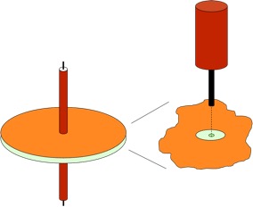
Figure 1: Via test structure
At least in the region between the two ground planes, this structure closely resembles a via, with the center conductor of the coaxial transmission line acting as the barrel of the via and the holes in the ground planes acting as the via antipads.
Note that in this structure, there is nothing that looks like a ground via. The only element providing continuity of the ground path is the coupling between the ground planes.
The experiment is to measure the insertion loss of this structure. Reflection coefficients can also be used to determine the impedance of the structure as a function of frequency.
The baseline structure for this study uses 0.062” thick FR4 dielectric, 4.5” outer diameter, and 0.117” holes in the ground planes (to match 141 semirigid coax cables at input and output). This set of dimensions was chosen for ease of fabrication at minimal cost using readily available materials and processes.
Note that the dimensions in the baseline structure are at least three times those used in typical printed circuit boards. The following table is a comparison of the relevant dimensions.
Table 1: Comparison of relevant dimensions
|
|
Experimental PC Board |
Typical Structure |
|
Via drill size |
0.036” |
0.012” |
|
Antipad diameter |
0.117” |
0.032” |
|
Dielectric thickness |
0.062” |
0.012” |
Thus, this sample is representative of the behavior to be expected in practice at three times the frequencies used in these measurements. This is an additional advantage for the dimensions chosen.
The circular symmetry of the baseline structure was chosen because a textbook solution was already available, and because the reonant frequencies of the structure are relatively evenly spaced, making it easier to interpret the data.
The methods of this paper can, however, also be applied to rectangular structures. Although the solutions are not necessarily available in a textbook, they actually easier to work with because they use exponentials rather than the Bessel functions required for circularly symmetric structures. Also, the resonant frequencies of a rectangular structure are typically not equally spaced, but rather tend to bunch up at higher frequencies. In practical PC boards, this can result in frequency bands or “suck outs” of perhaps several hundred Megahertz in which the loss is higher than expected.
1.2 Baseline Measurement
The S parameters of the baseline structure were measured using a vector network analyzer (VNA). A separate reference line using the same length of coax transmission line was also measured, and its insertion loss and reflection coefficient were subtracted from the data for the baseline structure. Figure 2 shows the resulting magnitude of S21 and S12 in dB’s. Both directions of transmission were included to provide some indication of the degree to which the data is reproducible.
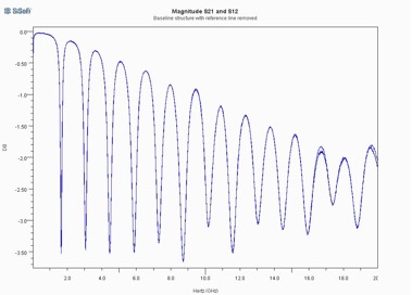
Figure 2: Baseline via structure S21
While there is certainly considerable distortion evident in Figure 2, the overall insertion loss is not necessary as high as one might expect for a structure with no ground vias. This is at least partially explained by the fact that the parallel plate capacitance of the ground planes is approximately 230pF; however, that capacitance is distributed over distances which can be several wavelengths, as is evident from the resonances in the structure’s response.
2.0 Physical Explanation
2.1 A Fundamental Theorem
Some insight can be gained into the behavior of this structure by considering the currents that flow at the edges of the ground plane holes and the currents in the center conductor. We will study these currents using Maxwell’s fourth equation which, in a very fundamental form, states that the integral of the magnetic field along a contour is proportional to the integral of the currents flowing through a surface bounded by that contour plus the time derivative of the electric flux through that surface.
Consider a contour defined around the hole in one of the ground planes and interior to the metal which forms that ground plane, as illustrated in Figure 3.
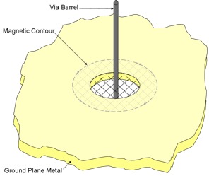
Figure 3: Magnetic contour inside ground plane metal layer
Then, for all frequencies for which the ground plane metalization is more than a few skin depths thick, the magnetic field in the interior of the metal, and therefore along this contour, is essentially zero.
Furthermore, if a surface bounded by this contour is defined in such a way that it covers the hole in the ground plane at exactly the middle of the metal thickness at the edge of the hole, then by symmetry, the electric fields at that surface will all be directed along the surface, and there will be no electric field flux penetrating the surface.
Therefore, considering that the integral of the magnetic field around the contour is zero and the electric flux through the surface (and therefore its time derivative) is zero, then the integral of all currents flowing through the surface must be zero.
This proves the theorem that for all frequencies for which the metal is many skin depths thick, the sum of all the currents flowing through a hole in a ground plane must be zero.
What this theorem implies is that if there is high frequency current flowing along the center conductor of the experimental structure or the barrel of a via, and that conductor passes through a hole in a ground plane, then there must be an equal and opposite current flowing back along the edges of the the hole. This condition is illustrated in Figure 4 for a via barrel passing through holes in two ground planes.
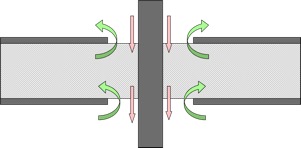
Figure 4: Currents related to a via barrel passing through holes in two ground planes
2.2 Radial TEM Waves
The above theorem can be used to explain how the experimental structure generates radial TEM waves. If there is a current flowing along the center conductor and into the cavity formed by the ground planes, then there must be an equal and opposite current flowing back along the interior of the cavity, through the hole in the ground plane, and back along the shield of the coax cable feeding the structure. Since the entire structure is radially symmetric, this current must be radially symmetric as well.
On the other side of the ground plane cavity, the current is flowing out along the center conductor and so there must be a radially symmetric current flowing through the hole in the opposite ground plane and into the cavity.
The currents at the edges of the ground plane holes are therefore equal in magnitude, opposite in sign, and radially symmetric. These currents therefore generate a circularly symmetric magnetic field, and an electric field is required perpendicular to the ground planes in order for the currents to flow in the first place. This, then, is a radial TEM wave. Energy flows away from and back to the holes in the ground planes like ripples in a pond, and both the electric and magnetic fields are perpendicular to the direction of energy flow.
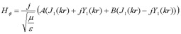
Reference [4] gives the following equations for radial TEM waves propagating between the two ground planes.
 (eq 1)
 (eq 2)
 (eq 3)
where
E is the electric field in the vertical direction
H is the magnetic field in the circumferential direction
A is the amplitude of a radial TEM wave propagating inward
B is the amplitude of a radial TEM wave propagating outward
k is a propagation number
r is the distance in the radial direction
Jn are Bessel functions of the first kind
Yn are Bessel function of the second kind
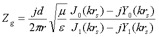
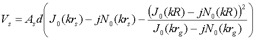
The resulting impedance between the two conducting planes with separation d between the two planes is
 (eq 4)
If there is only an outgoing wave, as would be the case for either an infinite plane pair or a matched impedance boundary condition surrounding the via, equations 1, 2 and 4 result in the ground impedance
 (eq 5)
where rs is the radius of the hole (antipad) in the ground planes.
If the planes have a finite outer radius R, then these equations can be solved by noting that the total current at the outer edge of the planes is zero.
 (eq 6)
Substituting the value for H from equation 2 into equation 6 and solving for B in terms of A,
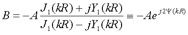 (eq 7)
Where the function psi is defined to observe that, at least in this lossless case, the magnitudes of A and B are the same, but that there is a phase difference between the two. This value for B can then be substituted back into equations 1 and 2, and those expressions can then be substituted into equation 4 to yield
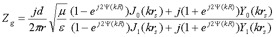 (eq 8)
Finally, the insertion loss due to this ground impedance when measured for a through path in a system with characteristic impedance Z0 is
 (eq 9)
Figure 5 shows the insertion loss these equations predict for the baseline structure if one assumes that the dielectric is lossless, and compares that loss to the measured data. In Figure 5, the measured data is colored blue and the calculated data is colored red. Note in Figure 5 that although the theoretical calculation produces a series of resonances which are similar to those of the measured data, only the first resonant frequency (~1.6 GHz) is matched exactly. As the frequency increases, the resonant frequencies from the lossless calculation become smaller and smaller compared to those for the measured data. Furthermore, the insertion loss predicted by the lossless calculation is lower than that for the measured data, except near the resonant frequencies. Thus, the treatment so far appears to be on the right track, but there is more physics to be accounted for.
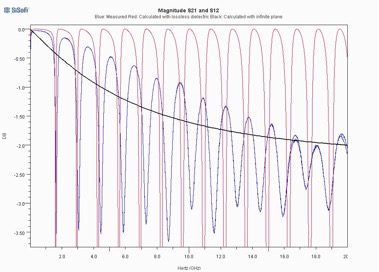
Figure 5: Theoretical predictions for lossless dielectric compared to measured data
Figure 5 also shows in black the insertion that would be obtained with an infinite ground plane or a matched absorbent boundary condition. The insertion loss for this case increases monotonically with frequency. Comparing the insertion loss curves, it’s clear that the waves reflected from the edge of the cavity play in important role in the behavior of the structure. This point should be considered carefully when applying a field solver to a structure like this. In particular, applying a matched boundary condition to the edges of the structure will cause the solver to miss phenomena which are central to the behavior of the via.
2.3 Lossy Dielectrics
It has been known for some time that losses in a dielectric will not only cause the dielectric constant to become a complex quantity, typically characterized by a loss tangent, but will cause the dielectric constant to decrease for increasing frequency. Djordjevic et al [5] describe the dielectric constant using the equation
 (eq 10)
where omega sub one is a lower frequency, typically 10 kHz, omega sub two is an upper frequency limit, typically 1 THz, sigma is the conductivity at DC, epsilon sub infinity is that dielectric constant at extremely high frequencies, and delta epsilon represents a relatively constant dielectric loss between omega sub one and omega sub two. For frequencies between these limits, the real and imaginary parts of the dielectric constant are
 (eq 11)
 (eq 12)
and the dielectric loss tangent is
 (eq 13)
for some omega sub zero located close to the middle for the frequency band of interest. For the types of dielectrics typically used in electronic systems, and for the degree to which the characteristics of these materials are typically controlled, we will assume that sigma equals zero (negligible DC leakage). Equation 10 therefore becomes
 (eq 14)
The effects of dielectric losses were taken into account through the simple expedient of substituting the complex value from equation 14 back into equations 3 and 8, and calculating the Bessel functions for complex arguments by adapting algorithms from [6].
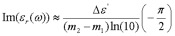
Figures 6 and 7 compare the magnitudes of S21 and S11 for the measured and calculations from equations 8, 9, and 14. For these calculations, different values for the loss tangent were tried until the resonant frequencies from the calculation agreed with the measured data. The dielectric loss tangent that resulted in the best match to the measured data was 0.040, which is much higher than that typically expected for FR4; however the materials for the experimental samples were obtained from a low cost, uncontrolled source. The correlation with measured data suggests that this is the correct value for this sample.
Note in Figures 6 and 7 that the frequencies of the resonances are matched quite well to 20 GHz, and that the magnitude of the return loss agrees quite well to 10 GHz. As observed in section 2.1 above, this corresponds to 60 GHz and 30 GHz, respectively, for most PC boards.
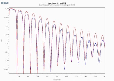
Figure 6: Comparison of measured to calculated S21 magnitude
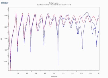
Figure 7: Comparison of measured to calculated S11
Note also that while dielectric losses account for most of the losses in the experimental sample, there are still some losses unaccounted for. These are most likely conduction losses in the ground planes. While it is beyond the scope of this paper to calculate the conductive losses in addition to the dielectric losses, it should be noted that while the voltage between the ground planes is proportional to the dielectric thickness, the voltage drop across the ground plane is independent of dielectric thickness. Therefore, conductive losses will become more important for thinner dielectric layers.
3.0 Differential Vias
The baseline experiment was extended to investigate the coupling between vias. Rather than having a single transmission line on either side of the ground plane structure and a single center conductor passing through the dielectric layer, samples were prepared with two closely spaced transmission lines on either side of the ground plane layer and two center conductors passing through the dielectric layer. To get a first order estimate of the effect of via spacing, two different samples were prepared: one with a spacing of 0.125” between center conductors in the dielectric layer and one with a spacing of 0.090”.
Figure 8 shows the measured insertion loss and return loss for both transmission lines in both directions. Note that these results are, in general, very similar to those in Figures 6 and 7.
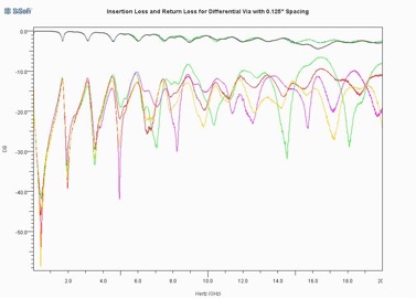
Figure 8: Insertion loss and return loss for differential via with 0.125” spacing
Figure 9 shows the crosstalk coupling between transmission lines for both transmission lines and both directions. There are several interesting observations that can be made about the data in Figure 9. First of all, note that the crosstalk coupling is, in general, quite high. This level of crosstalk would not be acceptable in a system application. Note also that the crosstalk coupling generally resembles the return loss shown in Figure 8. In point of fact, the two are almost exactly the same for frequencies below about 5 GHz. This suggests that the crosstalk coupling mechanism is a common ground impedance introduced by the ground plane structure, and that the same ground impedance is also the primary mechanism in the return loss.
Note also from Figure 9 that the magnitude of the crosstalk coupling is remarkably consistent between coupling paths, even at very high frequencies. This suggests that a differential via structure such as this may offer a very accurate way to measure via ground path impedance for more general ground plane shapes, in much the same way that a four point probe is used to measure resistance.
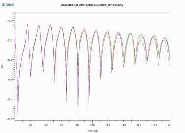
Figure 9: Crosstalk coupling for differential via with 0.125” spacing
Neither Figure 8 nor Figure 9 show the relative phase between the various responses. While we could have plotted the phases directly as well, it is much more instructive to transform the S parameters to differential and common mode. Figure 10 shows the differential mode insertion loss and return loss, while Figure 11 shows the common mode insertion loss and return loss.
Figure 10: Differential mode response of a differential via with 0.125” spacing
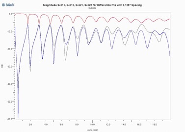
Figure 11: Common mode response of differential via with 0.125” spacing
Note that the differential mode response in Figure 10 is relatively well behaved while the common mode response is even more extreme than that for the single ended structure. This can be explained in terms of radial TEM waves in that for the differential mode, the radial TEM waves for the true and complement sides will nearly cancel each other out while for the common mode, the TEM waves add together in phase.
To provide some sense for the effect of via spacing, Figure 12 compares the differential mode insertion loss for the sample with 0.125” spacing to that for a sample with 0.090” spacing.
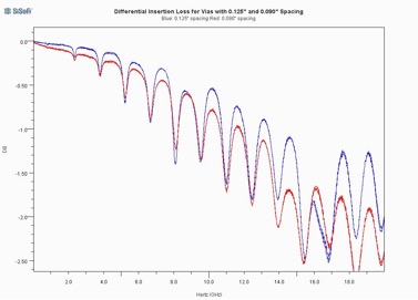
Figure 12: Differential insertion loss as a function of via spacing
In Figure 12, the 0.125” spacing is shown in blue and the 0.090” spacing is shown in red. Note that the insertion loss variation is greater for the larger spacing, indicating greater coupling to the radial TEM modes. This is what one would expect, in that the closer spacing results in more complete cancellation of the TEM waves.
It is possible to apply the methods of [1] and section 3.2 above to TEM modes which vary in the circumferential direction. The general behavior and resonant frequencies of the radial TEM mode which varies by one cycle in the circumferential direction agree quite well with the data in Figure 12. This also is consistent with the theory that the TEM waves from the true and complement sides cancel each other out almost, but not completely.
4.0 Ground Vias
Even recent and well respected books have suggested that there needs to be a lot of ground vias to provide a low impedance ground return path, and that these vias need to be placed as close as possible to the signal vias.
While this may be the case at frequencies for which the ground plane is less than a skin depth thick, it is not the case at higher frequencies, as demonstrated by the fundamental theorem above. Rather, at higher frequencies the ground return currents for each signal will find their way to the walls of the antipads associated with that signal, regardless of what is in between. A ground via may offer one path for that current, but the radial TEM waves offer another, much closer and more effective mechanism.
This principle can be demonstrated by extending the baseline experiment to include ground vias by drilling holes in the baseline structure so that grounding posts can be inserted or removed. Figure 13 shows the insertion loss for three different cases: no ground vias (shown in blue), four ground vias at a 0.800” radius from the center (shown in green), and an additional four ground vias at a 0.200” radius from the center (shown in red).
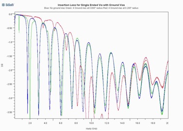
Figure 13: Insertion loss as a function of ground via spacing
The results are not necessarily what one would at first expect. While it is true that the grounding posts eliminate the resonance at DC, that is because the grounding vias are necessarily a very small number of wavelengths from the signal via near DC. At higher frequencies, the grounding posts have much less effect. There is a transition frequency band in which the ground vias shift the ground plane resonant frequencies and suppress the coupling to the ground plane resonances somewhat, but above that transition band, they have very little effect at all.
The grounding posts do have a greater effect when placed closer to the signal via; however, they have to be placed very close indeed to have any significant effect.
These observations can also be explained using radial TEM waves. Since the electric field at the walls of a grounding post must be zero, what happens is that the grounding post reflects radial TEM waves in response to incident TEM waves in such a way as to satisfy this boundary condition. These reflected TEM waves return to the signal via, where they subtract from the TEM waves emanating from the signal via.
- If the distance is small, then the amplitude and phase of the reflected wave will not have changed very much, and therefore the reflected wave will substantially reduce the voltage between the ground planes at the signal via.
- If, however, the ground via is at a greater distance, then its amplitude will decayed and its phase shifted, and so will have much less effect on the signal via.
- Finally, if the ground via is a quarter wavelength away from the signal via, then the reflected wave will be in phase with the wave emanating from the signal via, and will add constructively to it..
This principle can be readily demonstrated mathematically for the case of an infinite (i.e., very large) ground plane. If we define
As is the amplitude of the wave emanating from the signal via
Ag is the amplitude of the wave reflected from the ground via
d is the dielectric thickness
R is the distance from the signal via to the ground via
rs is the antipad radius of the signal via
rg is the radius of the ground via
Vs is the voltage at the signal via
Vg is the voltage at the ground via
then the boundary condition at the ground via is
 (eq 15)
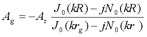 (eq 16)
Propagating the reflected wave back to the signal via,
 (eq 17)
Substituting equation 16 back into equation 17,
 (eq 18)
The case of a finite ground plane can be treated in much the same way except that since there are waves reflected from the edges of the plane as well as from the ground vias, the solution requires a matrix inversion, and so the solution does not illustrate the principle as clearly.
Measurements were also made with ground vias inserted in the differential via samples with the expectation that this would make other crosstalk mechanisms observable; however, the TEM wave suppression provided by these ground vias was not sufficient to expose any other physical phenomena.
5.0 Antipads
Section 3.1 demonstrates that the total current at the edge of the antipad is equal and opposite to the current flowing on the via barrel. Since the magnetic fields are directly proportional to these currents, the magnetic field at the edge of the antipad due to the ground currents is exactly canceled out by the magnetic field from the via barrel. Furthermore, the magnetic field due to the via barrel currents is due to a TEM wave propagating in the z direction, and so in the radial direction, the magnetic field is calculated using the static field solution. The magnetic field due to the via barrel is therefore inversely proportional to the radius.
These observations can be combined with the equation for the magnetic field due to the radial TEM waves (i.e., equations 2 and 7) to calculate the magnetic fields as a function of radius for the baseline structure.
Figure 14 shows the radial distribution of the magnetic field in the baseline experimental structure for frequencies ranging from 1 GHz to 20 GHz. This data demonstrates that at frequencies for which the antipad diameter is small compared to a wavelength, the magnetic field is almost entirely contained within the boundary of the antipad. When the antipad diameter starts to become a significant fraction of a wavelength, however, there is substantial magnetic field energy injected between the ground planes.
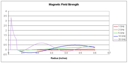
Figure 14: Radial distribution of magnetic field in baseline experimental structure
One would also expect the electric fields from the via barrel to terminate somewhere near the perimeter of the antipad, so that when the antipad diameter is small compared to a wavelength, essentially all of the fields are contained within the antipad boundary, and the via behaves like a short length of coaxial transmission line whose outer conductor diameter is the antipad diameter and whose center conductor diameter is the via barrel diameter. At higher frequencies, the leakage of the magnetic field between the ground planes will cause the via impedance to increase due to increased inductance, and for it to become lossier due to energy injected into radial TEM waves.
Thus, a good first order equivalent circuit for a single ended via is a coaxial transmission line with the radial TEM mode impedance in series with the ground. The radial TEM mode impedance can be calculated from equation 8 or, more generally, from [4], and the properties of the transmission line are
Dielectric constant and loss tangent the same as the dielectric layer.
Impedance defined by the antipad diameter, barrel diameter, and dielectric properties.
For a circular antipad and barrel, this is the
 (eq 19)
Length equal to the thickness of the dielectric layer.
If the antipad radius is comparable to or less than the dielectric thickness, this approximation will underestimate the impedance because the electric fields in the middle of the dielectric layer bend a bit past the projection of the antipad, making the effective outer diameter of the transmission line larger and therefore the effective impedance higher. For high density printed circuit board designs, this is typically not a significant consideration, however, because the board has so many layers, and so the first order approximation is more than adequate.
6.0 Conclusions
This paper introduces an experiment which demonstrates the role of radial TEM waves in the behavior of package and printed circuit board vias. Evaluation of closed form textbook equations gives good agreement with measured data. This paper then goes on to observe:
For differential vias, the radial TEM waves tend to cancel each other out, especially at lower frequencies, resulting in lower via losses.
Unless they are quite large and are placed quite close to the signal via, ground vias have only a small effect on signal propagation, except at frequencies for which the ground planes are less than a skin depth thick.
A first order equivalent circuit for a via is a transmission line with the impedance due to the radial TEM waves placed in series with the ground path.
References
[1] Schuster, Kwark, Selli and Muthana, “Developing a “Physical” Model for Vias”, DesignCon2006.
[2] Selli, Schuster, Kwark, Ritter and Drewniak, “Developing a “Physical” Model for Vias - Part II: Coupled and Ground Return Vias”, DesignCon2007.
[3] Archambeau, Connor, Araujo, Hashemi, Mittra, Schuster and Reuhli, “Full Wave Simulation and Validation of a Simple Via Structure”, DesignCon2006.
[4] Ramo, Whinnery and Van Duzer, Fields and Waves in Communications Electronics, Third Edition, Wiley, copyright 1994, pg. 464-71.
[5] Djordjevic, Biljic, Likar-Smiljanic and Sarkar, “Wideband Frequency-Domain Characterization of FR-4 and Time-Domain Causality”, IEEE Transactions on Electromagnetic Compatibility, Vol. 43, No. 4, pg. 662-7, November 2001.
[6] Press, Teukolsky, Vetterling and Flannery, Numerical Recipes in C++, third edition, Cambridge Press, copyright 2005, pg. 235-9.
For more information on this subject, please contact us at:
Signal Integrity Software, Inc (SiSoft)
6 Clock Tower Place, Suite 250 – Maynard, MA 01754
www.sisoft.com
978.461.0449