
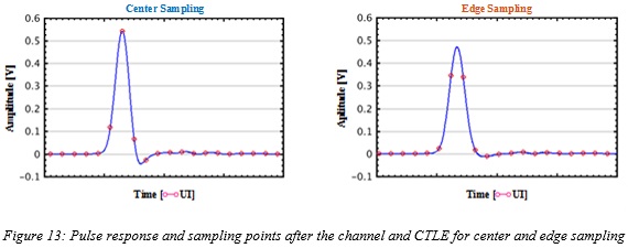
Pulse responses for center sampling and edge sampling with a 10dB channel loss are shown in Figure 13. The pulse responses are after the channel and CTLE and right before the sampling stage in the receiver. For the center sampling, it can be seen that there is one large center sample with other samples causing ISI. For the edge sampling, two identical sample values of smaller magnitude can be seen which construct the main three levels in the eye, with the remaining samples causing ISI. It is important to note that both of the pulse responses show the response with an optimal CTLE chosen for each scenario including ISI, crosstalk, nonlinearity, and noise.
The next step is to perform statistical simulations across a range of channel losses for both center and edge sampling and record the system performance. Figure 14 shows the vertical eye opening at a  for both sampling techniques. It can be seen that initially, at low losses
  , using a center sampling provides a better performance. However, as loss increases, since the bandwidth of the CTLE is limited by the technology parameters, edge sampling starts to become a more attractive option. For this example, the crossover point above which edge sampling outperforms center sampling is
  .
.

The analysis can be further expanded to also include the technology parameters as another degree of freedom. For example, the CTLE parasitic pole frequencies could be shifted to mimic advances in the technology or a tradeoff using additional power for a larger CTLE bandwidth. The analysis can then be completed for each value of the parasitic pole frequencies and to find the channel loss crossover point at which edge sampling outperforms center sampling.
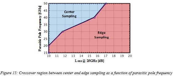
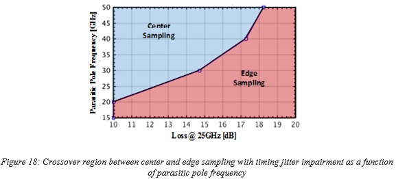
Figure 15 shows the regions where each sampling technique has a better performance. For each set of CTLE parasitic pole frequency, the channel loss is varied and the crossover is obtained. Depending on the technology parameters and the channel loss, an optimal choice can be made for the sampling scheme. For example, if the maximum pole frequencies are below 20GHz , then center sampling is always worse than edge sampling. However, if the pole frequency can be increased up to 50GHz , then center sampling has better performance than edge sampling up to 17dB of channel loss.
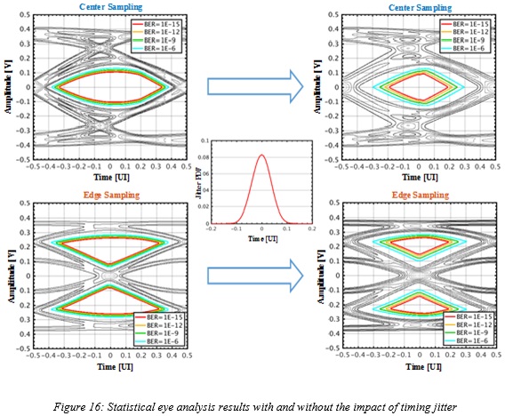
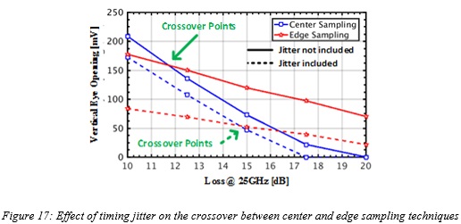
The analysis so far has only considered different sources of voltage impairments. In what follows, the effect of timing jitter is investigated and added to the statistical eye analysis. Jitter is generated in a time-domain simulation of the CDR as will be explained in the next section. The importance of including jitter in the analysis can be demonstrated as shown in Figure 16. The results are illustrated for a 10dB loss channel with CTLE parasitic pole frequencies of 30GHz.
Figure 16 shows the eye opening for each sampling scheme before and after the effect of jitter is modeled. An exemplary jitter histogram is also shown. A few main observations can be made from the simulation results. First, for both sampling techniques, the eye opening after jitter is included becomes smaller and better represents the actual system performance. Second, it can be seen that jitter has a different impact on each of the sampling techniques. There is a larger degradation in the performance for edge sampling after the effects of jitter are included due to the slope of the eye contours near crossing point in the middle of the eye. Therefore, if jitter is not included in the analysis, the wrong conclusion can be reached regarding the optimal sampling scheme. Statistical eye analysis appears to be a good approach for adequately quantifying the timing jitter on the eye closure, which as demonstrated here could have a detrimental effect on the performance.
The crossover analysis is repeated but this time looking at the vertical eye opening after the effects of voltage and timing impairments are considered. Figure 17 shows the new crossover point as a function of channel loss for a maximum CTLE pole frequency of 30GHz . It can be seen that the crossover point is now different and more in favor of center sampling. For example, edge sampling outperforms center sampling beyond  , however, if jitter was not included, the incorrect conclusion of would be inferred.
Finally, the analysis is performed for different maximum CTLE pole frequencies across different channel losses including jitter as shown in Figure 18. It can be seen that compared to Figure 15, the region where center sampling is the optimal solution has grown since edge sampling is more sensitive to the impact of jitter.
Clock Recovery
One of the key differences between the receiver architectures for center and edge sampling is the clock recovery. The clock recovery loop is responsible for adjusting the phase and frequency of the sampling clock to the sampling point at which the BER is minimum.
To compare different phase detector logics for center and edge sampling, the phase-interpolator (PI) based CDR architecture is chosen since it is the most popular architecture in advanced CMOS technologies. This is mainly because in PI-based CDRs phase detector (PD) and loop filter (LF) can be implemented in digital, so they benefit from technology scaling and are easier to port. Furthermore, the clock recovery phase-locked loop (PLL) can be shared between multiple receivers resulting in a lower power consumption.
Based on the PD logic, the number of required latches, serial-to-parallel converters (S2Ps), and PIs may vary. In this section, it is shown how the receiver architecture changes depending on the PD logic and the sampling technique. NRZ signaling is assumed here, but the results can be extended to multi-level schemes as well. For each one of the center and edge sampling techniques, two possible receiver architectures are considered: baud-rate sampling and 2x sampling.
Another degree of freedom in choosing the receiver architecture is the number of clock phases that are used to sample the incoming data. This is usually chosen based on the maximum clock frequency that can be achieved in a certain technology with reasonable power consumption. Here, the number of clock phases is considered to be R, resulting in an R -rate receiver. Half-rate ( R = 2 ) and quarter-rate ( R = 4 ) are the most common receiver architectures at  serial links.
Figure 19 shows a center sampling receiver using a bang-bang (BB) PD. The BB-PD ensures that the clock phase is set in such a way that  represent the edge samples from the received pulse response. Here, each received bit is sampled twice using two sets of latches, resulting in a 2x sampling architecture. The samples from center and edge latches go through serial-to-parallel conversion and the parallel data is sent to a digital core. The de-serialization ratio (N) is chosen based on the fastest frequency at which the digital core can operate. PD logic is applied to the parallel data to determine whether the clock signal is early or late compared to the ideal sampling point. This is achieved using the PD logic table shown in Figure 19.
A digital loop filter is applied to the early/late signals and usually includes integral and proportional paths. The output of the digital loop filter is the phase code that controls the phase of the clock signals in PIs. Since both edge and center clocks are required for the clock recovery, an offset is added to the output of the digital loop filter to generate the center clock that is typically half a UI apart from the edge clock.
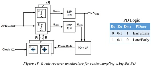
Figure 20 shows a center sampling receiver using a Mueller-Muller (MM) PD. The MM-PD ensures that the clock phase is set in such a way that  present the first pre-cursor and post-cursor samples from the received pulse response. Each received bit is sampled at one clock phase using three sets of latches. The data latches are responsible for both clock and data recovery but two sets of error latches are solely needed for clock recovery. The threshold of error latches are set to the main cursor of the received pulse response
  . The error signal can be
  depending on the outputs of the error latches.
Using the error and data signals and the PD logic table shown in Figure 20, early/late signals are generated. The rest of the clock recovery loop is similar to the architecture using BB-PD. It has to be noted that only one set of PIs is required in the receiver using MM-PD because all the latches operate on the same clock phase.

As for center sampling, the receiver architecture using MM-PD requires 1.5 times more latches and S2Ps compared to BB-PD, but it requires half the number of PIs. The receiver architecture using BB-PD does not require reference generators. The area and power of both architectures are very similar and one may have a slight advantage over the other subject to the technology and different circuit-level implementation details.
In terms of performance, the locking point using BB-PD is less sensitive to ISI in the channel. Also, setting the threshold voltages for the error latches in MM-PD may not be trivial. Therefore, the receiver architecture using BB-PD is usually preferred. It has to be noted that this argument is only true for mixed-signal receivers. In case of ADC-based receivers, MM-PD consumes less area and power since it does not require any additional latches or S2Ps for clock recovery due to the presence of an ADC.
Figure 21 shows an edge sampling receiver architecture using BB-PD. Assuming pre-coding in the transmitter, the data in the receiver can be recovered using two sets of data latches and a simple XOR gate. This implements the memory-less modulo 2 detection of the pre-coded NZR signal explained earlier.
The blocks solely used for data recovery are shown in gray color. Note that the data recovery may change if there is no pre-coding in the transmitter, but the clock recovery will remain the same. To recover the clock using BB-PD, two sets of center and edge latches are needed. Since the latches and S2Ps cannot be shared between clock and data recovery paths, the edge sampling receiver architecture using BB-PD consumes more power and area compared to the center sampling receiver.
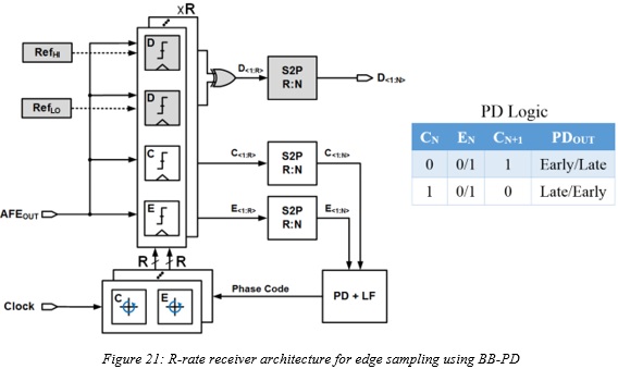
Figure 22 shows an edge sampling receiver architecture using edge locking (EL) PD. The EL-PD requires one sample per UI to set clock phase in such a way that  represent two neighboring equal cursors in the received pulse response. Each received symbol is sampled at one clock phase using three sets of latches. Two sets of data latches and one set of sign latches are needed for clock recovery. The same data latches can be used for data recovery if there is pre-coding in the transmitter. The data signal can be
  depending on the outputs of the data latches. The data and sign signals are used to detect the received pattern and extract the phase information using the PD logic table shown in Figure 22.
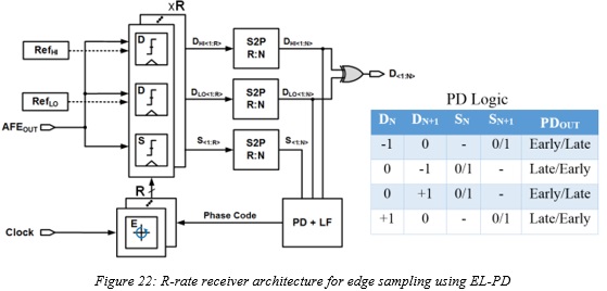
As for edge sampling, the receiver architecture using BB-PD requires 1.25 times more latches and 2 times the number of PIs compared to EL-PD. Therefore, in terms of area and power, EL-PD outperforms BB-PD. In terms of performance, the EL-PD has similar problems to the MM-PD for center sampling such as sensitivity to ISI in the channel and the threshold voltages for the data latches. Although, data latches are needed for data detection and cannot be avoided.
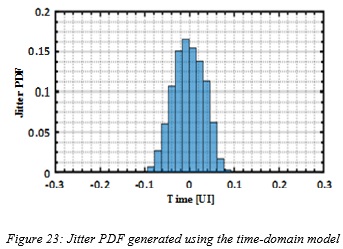
To compare the performance of center and edge sampling, a cycle-accurate bit-true time-domain model was built in MATLAB Simulink. The model incorporates various timing impairments such as power supply induced jitter (PSIJ), random jitter (RJ), nonlinearity in PIs, duty cycle distortion (DCD), skew between clock signals in multi-phase transceivers, and bang-bang jitter due to the CDR loop dynamic. The time-domain model was used to generate probability distribution function (PDF) of jitter in order to be employed by the statistical model to accurately predict the system performance including all timing and voltage impairments. Figure 23 shows an example of the jitter PDF generated using the time-domain model.
Optimum Slicing Threshold
Once the sampling clock phase is aligned with the desired sampling point, the task of signal detection becomes a matter of slicing the signal at optimum threshold levels. This task may be integrated within the CDR, as mentioned before, or left to a later stage in other implementation alterations. Although slicing the signal at any point inside the target BER eye contour is a possibility, placing the slicing thresholds at their optimum levels provide maximum margin and minimizes BER.
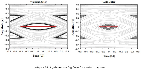
While the trivial choice of the optimum threshold level for center sampling is at the midpoint of the eye opening contour, the choice may not be so trivial for edge sampling. Optimality of midpoint slicing of the center samples stems from the fact that the eye opening is vertically symmetric at its center point. As a result, midpoint slicing provides an optimum unbiased decision outcome, regardless of the impairments and as long as the impairments also constitute unbiased voltage deviations (zero mean).
This is illustrated in Figure 24, where statistical eye analysis has been performed at various BERs for an example channel and impairment conditions to generate the trajectory of the optimum slicing level as the eye contour reaches its minimum opening for the lowest BER target. Trajectories are generated for two cases of with and without timing jitter impairment.
Optimum slicing levels in edge sampling could be affected by timing jitter. This is due to the influence of the vertical asymmetry of the eye opening at its edge point. The asymmetry causes more voltage variation around the eye contour where the contour has a steeper slope. As a result, depending on the purpose of margining, the optimum slicing level may or may not be centered.
If the reason for margining is to maximize the performance margin against voltage impairments, then the threshold levels should continue to be placed at the midpoints of the vertical opening of the edge eyes. However, if there is a desire to include the effect of timing perturbations on the margining, then the optimum threshold should be more distanced from the steeper slope side of the eye contour. In a practical solution, this decision may be weighted between margining for voltage impairments and timing impairments.
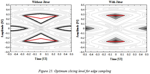
Figure 25 shows the result of statistical eye analysis on the same above channel and impairment conditions example used for center sampling, where trajectories of the optimum threshold levels for the edge eye openings are plotted as BER varies. Note that as expected, and unlike center sampling, in the presence of jitter margining the optimum threshold levels are no-longer placed at the vertical midpoints of the eye openings. Also note that while without jitter edge sampling outperforms in this example, the effect of jitter on its performance is more detrimental than center sampling and causes a complete eye closure even before the minimum BER target is achieved.
Conclusion
The ability to optimize a transceiver implementation depends on the thoroughness and accuracy during the process of architectural decisions. In this paper, a modeling and analysis methodology was proposed to evaluate the performances of center and edge sampling schemes based on statistical eye analysis. By adequately representing and modeling the voltage and timing impairments, the analysis demonstrated that the choice between center and edge sampling is not a trivial one and deserves proper attention for demanding high data-rate wireline applications.
The findings pointed to the existence of a performance crossover point between center and edge sampling schemes. Statistical eye analysis was shown to be an adequate tool to quantify this crossover point and help the system architect early in the design phase and before much effort is put in running long and time-consuming simulations. Finally, note that using binary NRZ signaling in most of the examples given here was for illustration purposes and the methodology and general conclusions similarly apply to any M-PAM scheme.
An earlier version of this article was a Best Paper Award Winner at DesignCon 2019.
References
- D. G. Kam, T. J. Beukema, Y. H. Kwark, L. Shan, X. Gu, P. K. Pepeljugoski, M. B. Ritter, “Multi-level Signaling in High-density, High-speed Electrical Links”, DesignCon 2008.
- T. D. Keulenaer, J. D. Geest, G. Torfs, J. Bauwelinck, Y. Ban, J. Sinsky, B. Kozicki, “56+ Gb/s Serial Transmission using Duobinary Signaling”, DesignCon 2015.
- J. V. Kerrebrouck, T. D. Keulenaer, J. D. Geest, R. Pierco, R. Vaernewyck, A. Vyncke, M. Fogg, M. Rengarajan, G. Torfs, J. Bauwelinck “100 Gb/s Serial Transmission over Copper Using Duo-binary Signaling” DesignCon 2016.
- CEI OIF Standards, “CEI-56G-XSR-PAM4”, “CEI-56G-VSR-PAM4”, “CEI-56G-MR-PAM4”, and “CEI-56G-LR-PAM4”.
- K. Mueller and M. Muller, "Timing Recovery in Digital Synchronous Data Receivers," IEEE Transactions on Communications, vol. 24, no. 5, pp. 516-531, May 1976.
- J. D. H. Alexander, "Clock recovery from random binary signals," Electronics Letters, vol. 11, no. 22, pp. 541-542, 30 October 1975.
- P. Kabal and S. Pasupathy, “Partial-Response Signaling,” IEEE Transactions on Communications, vol. 23, no. 9, pp 921-934, September 1975.
- A. Lender, "The Duobinary Technique for High-Speed Data Transmission," Transactions of the American Institute of Electrical Engineers, Part I: Communication and Electronics, vol. 82, no. 2, pp. 214-218, May 1963.
- J. G. Proakis and M. Salehi, "Digital Communications," McGraw-Hill, 5th Edition, 2008.
- G. D. Forney, Jr., "Maximum-Likelihood Sequence Estimation of Digital Sequences in the Presence of Intersymbol Interference," IEEE Transactions on Information Theory, vol. 18, no. 3, pp. 363-378, May 1972.
- M. H. Shakiba, “Analog Viterbi Detection for Partial-Response Signaling,” Ph.D. Dissertation, Department of Electrical and Computer Engineering, University of Toronto, 1997.