
Printed circuit boards (PCBs) are becoming ever-more crowded while designs in which they are used use more complex RF signaling. While impedance measurements have always been important, they have become even more so with these emerging designs. To ensure the signals correctly propagate through the board, a vector network analyzer (VNA) equipped with time domain analysis that includes basic and advanced window and gating functionality can help produce more accurate and repeatable impedance measurements.
Time domain data is valuable when conducting PCB measurements because it provides insight on a device under test (DUT) that is missing in the frequency domain. A VNA offers several benefits for time domain measurements, including:
- In-frequency response for accurate insertion and return loss analysis
- Multiple calibration methods to ensure accurate measurements
- Embed and de-embed capabilities
A VNA with a wide bandwidth, such as the VectorStar™ ME7838 Broadband Series, provides enhanced resolution in time domain compared to time domain reflectometry equipment. This is particularly important for emerging high-frequency designs. The wider the frequency coverage of the VNA, the better time domain resolution can be achieved. The resolution is particularly important to find defects and other anomalies in a system.
Transferring Date from Frequency Domain to Time Domain
A key aspect of using a VNA for impedance measurements is to use Inverse Discrete Fourier Transformation (IDFT) to transfer frequency domain data into time domain to create time domain samples. When converting to time domain using IDFT, the VNA becomes a periodic function, offsetting the inherent band-limiting nature of the instrument. Figure 1 shows a periodic impulse response in the time domain using a VNA integrating IDFT. The two vertical lines show the free alias zone from -25 ms to +25 ms.

Free alias zone |
Periodic impulse response in time domain |
Figure 1. Periodic impulse response in time domain using a VNA with IDFT.
Signal integrity engineers can select two types of time domain when using a VNA:
Low Pass Time Domain – The VNA can simulate a TDR with a step stimulus with this option. An impulse stimulus can also be applied, so engineers can view impulse responses in the time domain. Frequencies must be harmonically related, i.e., the start frequency must equal the step size. The DC term is extrapolated from the lowest frequency value. One factor to consider is that frequency samples double from negative frequency to positive frequency to meet the IDFT requirement when using the low pass time domain.
Band Pass Time Domain – To locate faults along the transmission lines, band pass time domain is recommended as arbitrary start and stop frequencies can be set. Considerations with this method include the fact that there is no DC item and resolution is less, compared to the low pass time domain mode. After IDFT is the impulse response is no longer a real function as well.
Figure 2 shows how measurement results will vary, depending on which time domain type is used. Determining which is a best depends on the testing requirements associated with the design.
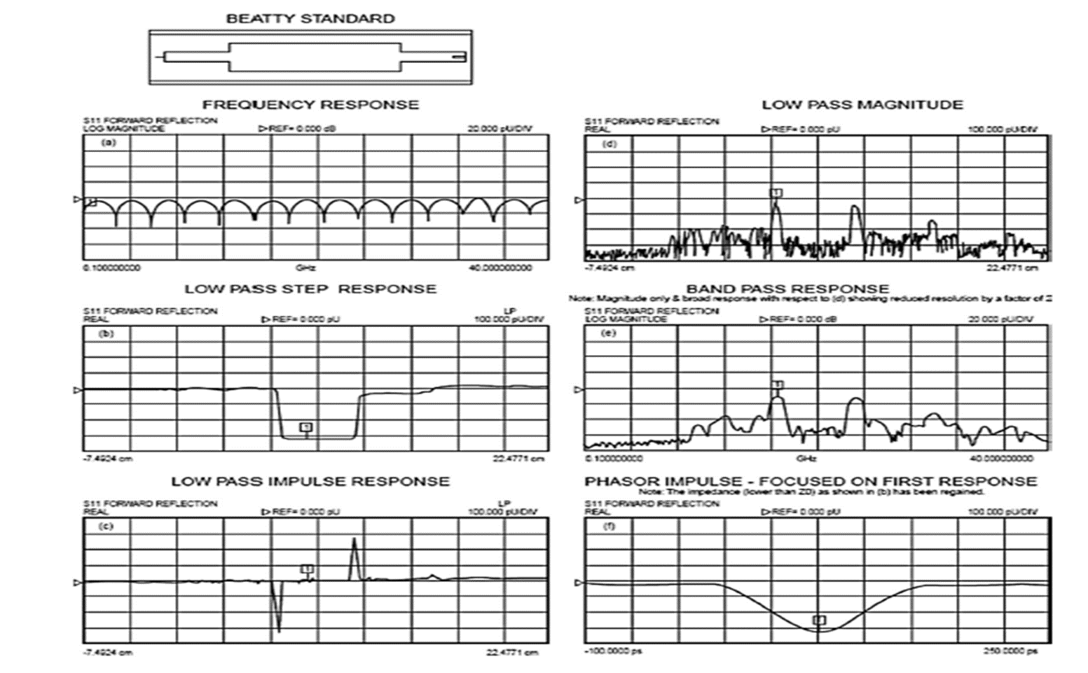
Figure 2. Examples of low pass and band pass time domain measurements.
Reflection Coefficient Representation of Transmission Lines
Impedance observed at the terminals of a transmission line has a more complicated dependence on the termination. For this reason, the relation between the impedance at the "generator" terminals and the impedance of the "load" should be measured. This is referred to as the reflection coefficient, representation of transmission lines.
A VNA is an ideal instrument to measure the reflection coefficient of a transmission line with multiple discontinuities. It converts the reflection coefficient at a discontinuity in impedance format in step response under low pass time domain, or it can display the discontinuities’ real format in impulse response under either low pass time domain or bandpass time domain.
Figure 3 is an example of having three different impedances on the transmission line and an equation to perform the calculation of the reflection coefficient at each discontinuity interface. The VNA measurement can relate well with theoretical calculation. In an example of an airline Beatty line measurement, the measured value of the first reflection coefficient is -0.331 vs. the theoretical calculated value of -0.333, and the second reflection coefficient at the second discontinuity interface measured .288 vs. the calculated theoretical value of 0.296. The slight discrepancy is the result of the energy loss along the Beatty line.

Figure 3. Determining reflection coefficient representation of transmission lines is valuable when measuring PCB performance.
Window Functions Impact on Resolution
A window function is a valuable feature that can make measurements more efficient and improve accuracy, as it mitigates frequency extremes in frequency domain and observes the effect in time domain. Certain VNAs offer a window function to correct ringing that can occur when the measurement is converted to time domain.
The window is a curve derived from a mathematical function that tapers off from unity gain at the center of the frequency domain data to a low value at the ends. This is not without a price, since the window has the effect of widening the main lobe, thus decreasing the effective resolution. For this reason, it is good to have a range of different window types available, so multiple views between resolution and side lobe effects – determined by the application – can be used.
As noted, windowing can have an adverse impact on effective resolution. To create the best possible resolution, a rectangular feature can be used in the frequency domain. Higher resolution equates to faster risetime. The trade-off is large side lobes, which can create larger ringing. Side lobes are an issue when identifying multiple reflection centers on a DUT. In these scenarios, a low side lobes window function is ideal. If the DUT has small reflection at the band edge, such as an airline with a termination at the end, a higher resolution is favored. Figure 4 is a display utilizing the rectangular feature and associated side lobes.

Figure 4. A measurement displaying highlighting the impact of a VNA utilizing the rectangular feature to improve resolution.
Time Domain Gating in VNA
Another effective tool when measuring impedance is a gating function. The gate is essentially a filter in the time domain to remove a specific discontinuity, such as a test fixture, cable, or connector. With any imperfection removed, truer measurements on the performance of a microwave circuit can be achieved. Certain VNAs allow users to easily control different gating functions and their width to observe the gated frequency response, as well as the time gated response.
Because this unnecessary data is not acquired in the measurement, errors, or ripple in the frequency domain response are eliminated. As in windowing, VNAs need to provide a choice of gate functions so the user can select the best trade-off of resolution versus ripple.
Results are displayed in the frequency domain. Multiplying a gating window function in a time domain response and converting it to frequency domain by Discrete Fourier Transformation allows the gated frequency response or impedance to be viewed and analyzed with greater detail.
Conclusion
In emerging, high-frequency PCB designs, a VNA has the ability to cost-effectively measure impedance with high accuracy and repeatability. Certain features, including window functions and time domain gating, provide the detailed analysis required for engineers to have confidence in their designs.