This plot of line width and gap separation to achieve a target impedance of 100 ohms defines design space for this differential pair, given its other parameter values. As long as the design always “walks this line,” the differential impedance is constant. This principle of defining design space for a fixed target impedance and constraining the differential pair design to this plotted line is referred to as the Johnny Cash Principle, after his first gold album, “I Walk the Line.”
The Johnny Cash Principle is important when routing a differential pair through a constrained region such as a connector or BGA via field. As long as the differential pair always “walks the line,” the differential impedance will be constant for any gap separation. There will be no impedance discontinuity even if the line width and gap separation change, consistent with the design space.
For example, in the case of 1 oz copper traces, a line width of 1 mil and gap separation 1.5 mils could be used in a via field and then expanded out to 3 mil wide traces and a gap separation of 8 mils in a less congested region of the board. The differential impedance would be perfectly constant.
Alternatively, a differential pair with a line width of 6 u and gap of 6 u starts as 100 Ohms. These features would allow four routing channels from a 0.5 mm pitch BGA pad field. An example of routing four tracks in a BGA field while the trace width and gap are adjusted to walk the line, is shown in Figure 5. These features would dramatically simplify routing from dense via fields.

Figure 5. An example of the routing of a 100 ohm differential pair with four routing tracks between 0.5 mm pitch BGA pads, adjusting the trace cross section to "walk the line." Ultra-fine lines, 6 u line width, and 6 u gap, enable fitting four tracks between the pads. This dramatically simplifies the routing requirements for large BGA devices, while maintaining a constant 100 ohm differential impedance.
Impact from Conductor Thickness
Of course, the specific values of the differential impedance will also depend on the conductor thickness. When all terms are fixed, a thicker conductor will result in a lower differential impedance, but not by much. The conductor thickness will affect the design space for line width and gap separation. Figure 6 shows the same design space for gap separation and line width for the four different thicknesses of 17 um, 34 um, 51 um, and 68 um.
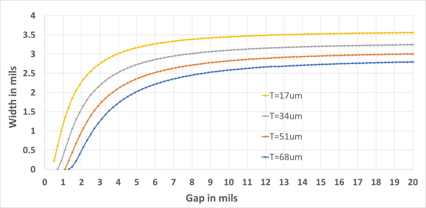
Figure 6. Design space for 100-ohm differential impedance for four different conductor thickness from 1/2 oz to 2 oz copper. Each curve is a line of constant 100-ohm differential impedance.
When the gap separation becomes large enough there is no coupling between the two traces in the differential pair. The differential impedance is no longer dependent on the gap separation when you reach this limit. The line width reaches a constant value at large gap separation, even as the gap separation changes.
The thicker the conductor, the lower the differential impedance. For thicker conductors, the line width would need to be narrower to maintain the same 100 ohm differential impedance.
By sweeping multiple parameters and finding the values for the other parameters that results in the target impedance, pairs of parameters can be analyzed to see the trends. This helps build design intuition and provides a starting place to find the optimized set of parameters based on material availability, manufacturing capability, and design constraints.
A New Metric for the Channel Width
When the impact on differential impedance from design parameters is displayed, it is customary to use the inside gap between the lines that make up the pair as a metric of the coupling between traces in a differential pair. After all, this is a metric for the extent of the fringe fields. However, a more interesting metric is the span of the differential pair: the outside edge to outside edge distance in a differential pair. This defines the total width the channel takes up on the board. This was illustrated in Figure 2.
The span of a differential pair is one metric that describes the extent of the differential pair on a board. When determining how to fit a differential pair through a dense via field, the span is a useful metric. It defines how wide a path the differential pair needs.
In an open routing field, the density of channels, or the pitch between channels, is driven by the acceptable level of crosstalk which strongly depends on the outside edge gap separation between two adjacent differential pairs. This crosstalk analysis is covered in a follow-on paper in this study. The routing pitch of a differential pair, limited by cross talk, is the span of the differential pair plus the acceptable adjacent channel to channel gap.
The span is the sum of the gap separation and 2x the line width. When all the other parameters are fixed, the span is a unique parameter for design space. For a fixed span, there is only one combination of line width and gap separation that achieves a target differential impedance.
For example, Figure 7 shows the differential impedance for a pair with a fixed span of 5 mils as the line width changes. As the line width decreases, the gap separation will increase to keep the span fixed. This will increase the differential impedance. For a fixed span, only one combination of line width and separation will result in the target impedance of 100 ohms. For example, for a span of 5 mils, when the line width is 1.8 mils, the gap is about 1.4 mils, and the differential impedance is about 100 ohms for 0.5 oz copper traces.
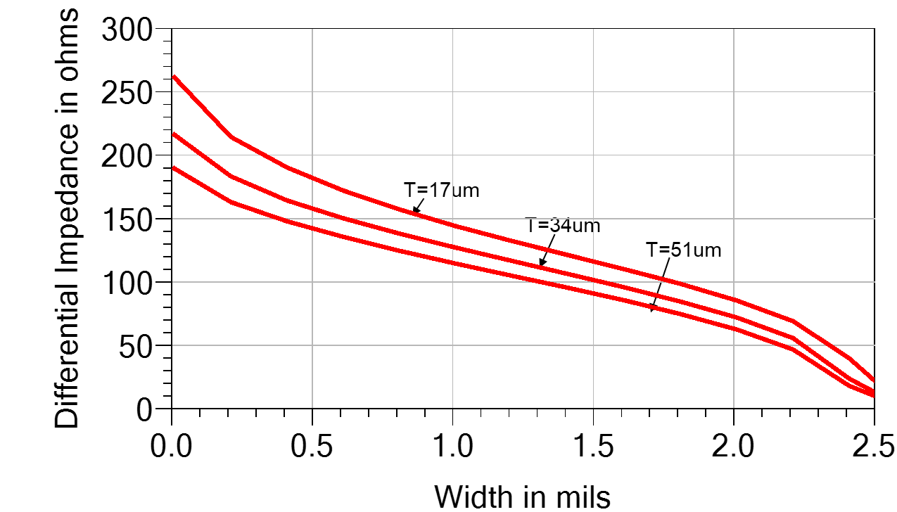
Figure 7. The differential impedance of a pair with a fixed span of 5 mils. There is one value of line width and gap separation that results in a specific target impedance.
Design Space for Differential Pairs in Terms of Span
Using this new metric of the span, we can explore design space for a differential pair. As the span increases, the design space for the linewidth and span for a 100 ohm target impedance is shown in Figure 8.
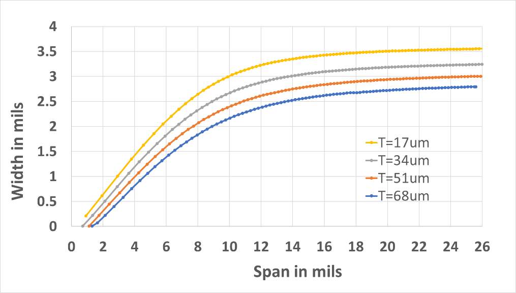
Figure 8. Design space for a 100 ohm differential microstrip showing the line width for a trace as the span is changed, for four different conductor thicknesses.
As the span increases, there is a limit to the line width needed to achieve a target impedance. This is for the same reason we found in the case of sweeping the separation. As coupling between the pair is reduced, the differential impedance is defined only by the line width, trace thickness, and dielectric thickness. There are no contributions from coupling to an adjacent trace.
There is a small impact from the trace thickness. When the span is large and the gap is large, the thicker conductor adds more fringe fields from the trace side wall which would decrease the differential impedance. This requires a narrower line to meet the 100 ohm differential impedance target.
Conclusion
A differential pair transmission line has many parameters that influence its differential impedance. We presented a methodology to systematically explore the design constraints to achieve a target impedance using a 2D field solver.
When all other parameters such as dielectric thickness and conductor thickness are fixed, the Johnny Cash Principle defines the constraint between line width and either gap separation or span to achieve a target impedance. As long as the differential pair is consistent with this constraint, the differential impedance will be constant, as the differential pair makes its way from inside a via escape field to a less confined open routing field.
We introduced a new parameter, the span of the differential pair, which localized the space required to route a differential pair through a constrained via field.
With the recent introduction of the Averatek Semi-Additive Process (A-SAP™) process, an engineer can now design a differential pair that can fit within an 18 u span enabling four routing traces in a dense via field and expand to a wider trace and span in a less dense region, all at constant differential impedance.
References
Eric Bogatin. 2021. “New Electroless Process Promises Finer PCB Features.” Signal Integrity Journal. https://www.signalintegrityjournal.com/blogs/4-eric-bogatin-signal-integrity-journal-technical-editor/post/2122-new-electroless-process-promises-finer-pcb-features
Eric Bogatin, Chaithra Suresh, Melinda Piket-May, Haris Basit, Paul Dennig. 2022. “Utilizing Fine Line PCBs with High Density BGAs.” Signal Integrity Journal. https://www.signalintegrityjournal.com/articles/2386-utilizing-fine-line-pcbs-with-high-density-bgas