
Electrostatic discharge (ESD) is one of those nasty things that can wreak havoc on portable and other electronic products. Manufacturers must build in protection against current from these high-voltage pulse discharges. This is especially important for I/O and power connectors, as well as any exposed metal in the user interface. Previously, I described several methods for simulating and detecting ESD. Now, we'll discuss how to troubleshoot an ESD failure.
ESD is a challenging product failure to debug. Part of the reason for this is the intermittent nature of the discharges. To help correlate circuit disruption with ESD, I use a simple ESD detector circuit you can build, to detect events when they occur.
Most designers end up trying to troubleshoot ESD at the compliance test lab. The drawback is that troubleshooting in this environment is time-consuming and expensive. It also greatly delays product introduction. Wouldn't it be nice to move this troubleshooting process onto your own workbench? Read on!
Even when troubleshooting in a controlled test environment, it’s difficult to know precisely what part of the circuitry or system is being affected, nor is it clear what path the ESD current actually takes. This is especially an issue with medium to large systems.
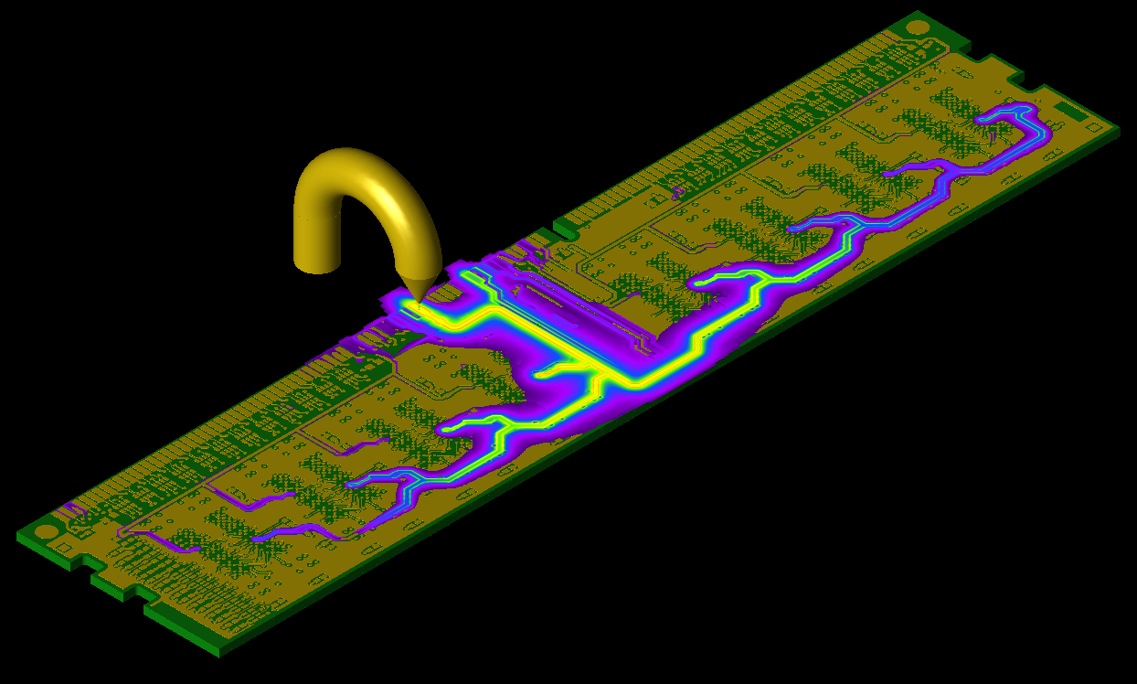 Figure 1. A simulation of injected ESD current onto a DDR RAM module using XFdtd. (Image courtesy of Remcom Inc.).
As can be observed in Figure 1, the path of ESD current can take several directions, based upon the paths of lowest impedance. Eventually, the current will return back to earth and to the human or object that created the discharge in the first place.
Tracing ESD Current Paths with the HP547A
Unfortunately, it’s not possible to see these current pathways or deduce what electrical components or active devices may be affected, causing product compliance failure. However, one method that has worked well in tracing out the discharge path is to inject low-voltage pulses from an ESD simulator into failure points on a product, or system, and then trace the path(s) using something like the HP 547A current tracer or simply a medium-sized H-field probe.
In the mid-1970s, HP developed a set of three handheld probes: a logic probe (HP 545A), a current pulser (HP 546A), and a current tracer [1]. These were replaced later with the updated HP 10525T logic probe and 10526T pulser sold together as the HP 5015T Logic Troubleshooting Kit. As far as I know, the current tracer was not upgraded. The combination of current pulser and current tracer were originally meant to locate shorts or latch-ups in complimentary metal-oxide semiconductor (CMOS) and high-density CMOS (HCMOS) circuits, circuit board shorts, and so forth.
From the original user manual [2]:
The HP 547A current tracer is a handheld probe which enables the precise localization of low impedance faults in electrical systems. The probe senses the magnetic field generated by a pulsing current internal to the circuit or by current pulses supplied by an external stimulus such as the HP 546A or 10526T Logic Pulsers. Indication of the presence of current pulses is provided by lighting the indicator lamp near the current tracer tip. Adjustment of probe sensitivity over a 1 mA to 1 A range is provided by the SENSITIVITY control near the indicator.
The current tracer (Figure 2) can accept power from 4.5 VDC to 18 VDC and comes with small finger-operated grabber clips for attaching to the circuit under test. I typically cut off the connectors and connect the two wires to proper banana plugs, as the grabber clips were kind of finicky to use. Some used probes don’t include the grabbers, but that’s probably not a great loss.
I found a complete set of these several years ago on eBay and wondered how to use them, especially the current tracer, in my EMC consulting to track down damaging current flowing from ESD events, especially for complex systems with multiple circuit boards, power supplies, and cables. 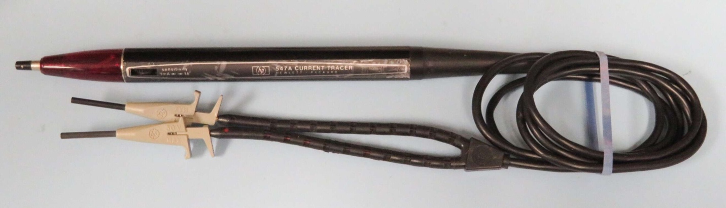 Figure 2. The HP 547A current tracer probe comes with two clips that I’ll replace with banana plugs.
I soon had an opportunity to try out the technique. One of my medical product clients called for help with an ESD compliance failure that had kept them busy for some weeks trying to troubleshoot. The system was a desk-standing electro-mechanical system with a main circuit board and power supply, a keyboard and display board, several solenoid actuators, and numerous interconnecting cables.
Injecting ESD at anywhere from 2 kV to 15 kV caused an actuator to fire at the wrong time. The system was particularly sensitive at the two side-enclosure panels near the front.
After doing a fair amount of troubleshooting and applying potential fixes, we were getting close, but still not sufficient to meet the new 15 kV requirement per the IEC 60601-2 standard. Part of the issue was the keyboard and display, which were poorly bonded to the enclosure. Furthermore, numerous system cables could have been related to the problem.
After some head-scratching (and some lunch), I pulled out the current tracer, set it to 1 A sensitivity and connected it up to an external 12 V power supply. We then turned the system on its side and injected a small 500 V ESD pulse into one of the sensitive areas. As my client applied repeated pulses every few seconds, I started probing around on the keyboard/display board and cables (Figure 3).
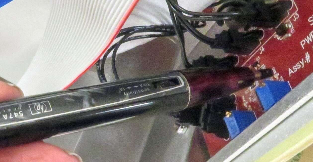 Figure 3. The HP 547A current tracer in use. We were able to isolate the dominant path of ESD current quickly by probing different cables and areas on the keyboard/display board.
The lamp brightness indicated the relative amplitude (and dominant path) of injected ESD current pulse. We were easily able to isolate the path of ESD to just a few of the cables as well as the display and controller board. It turned out the bulk of the ESD current was crossing through the IC that controlled the solenoids. Now we could try various bonding and shielding methods to see the result in near real time.
Between properly bonding the keyboard/display to the chassis, rerouting cables to the solenoids, and adding one ferrite choke, we were able to achieve 15 kV compliance.
There are other more modern current tracers available, but it seems their probe tips are rather large and may not work in this type of application. The HP 547A has a very small tip and is sensitive enough to detect low-level ESD. I found it perfect and easy to use for this type application.
Current tracer probes were more prevalent 10 years ago, but occasionally I see them pop up on eBay or other surplus outfits for $50 to $100. This just might be the right tool for those really difficult ESD challenges, and I plan to keep this in my troubleshooting kit. I wrote an article on how to use these for troubleshooting [3].
Tracing the Path of ESD with an H-field Probe and Oscilloscope
Because the HP 547A current tracer probe may be difficult to find, an equally simple method is to use an oscilloscope and small H-field probe to trace the dominant path of current, plus all its branches.
In one method, an assistant holds the simulator and triggers it repeatedly into one of the failure points, while another traces the dominant injected currents. If your simulator has a setting for one pulse per second, that would work as well and requires only one person. Generally, the equipment under test (EUT) will need to be opened up to reveal the internal circuitry and system cabling during this test. Figure 4 shows a block diagram of the test setup.
 Figure 4. Typical test setup to inject ESD current pulses and trace the paths of current flow.
These paths will commonly include system cables, PC boards, keyboards, and displays. The controlled discharges can be traced with the H-field probe by coupling the probe to cables or sweeping the probe around circuit boards. If the current pulse crosses through an IC, or other active device, that should provide a good clue as to the portion of circuitry that is involved with the failure mode of the product or system under test.
For example, let's assume discharging to a particular I/O connector shell on the EUT causes circuit upset during the ESD test. We'll want to connect the discharge tip to this connector ground shell to trace the path the ESD current is taking.
To illustrate this technique, we'll use a demonstration circuit board (Figures 5 and 6) and connect the simulator contact discharge tip to the I/O connector shell in question using a short clip lead. For the purposes of this demonstration, a drain wire at the power connector needs to be connected back to the ground return plane on the test table to provide a discharge path for the ESD current. The best location for this would be where the board normally connects to the power return.
Usually, you’ll be testing a whole system with the return path being the power cable earth connection. In that case, there’s no need to add a return wire to the circuit board ground return plane.
For portable products, it gets a little more complicated. You may need to use the equivalent of an “artificial hand” that will help bleed off charge for each ESD injection. Alternatively, you might connect a short wire with a series 100 k? power resistor between the power connector ground and ground return plane.
Start by setting up the oscilloscope for 200 mV per division, time base at about 8 ns per division, and use Auto acquisition. Plug the H-field probe into channel one and set the input impedance to 50 ?. You may need to adjust the trigger control slightly positive to catch each pulse. These initial settings are not critical and can be refined during the testing.
Adjust the ESD simulator for an automatic one pulse per second discharge rate (or have an assistant apply pulse on demand). Then, scan the H-field probe around the board to determine the path or paths by observing the relative pulse amplitude. The board does not necessarily need to be powered for this test, but if line-powered, should be plugged in to power to allow ESD currents to return to earth. Figures 5 and 6 show the general setup and tracing technique.
Since intense transient electric and magnetic fields are created by the discharge into the EUT, it is very important to ensure that the probe setup is not picking up the radiated fields created by the discharge. It is very easy to confuse any radiated energy picked up by the probe as the current on the ESD path and it can lead you to a wrong solution.
I use the medium-sized H-field probe and a minimal 100 to 500 V ESD injection to minimize this coupling. Always perform a “null” test with the probe in the air near the system under test to assess the amount of radiated field pickup, if any, and compare that level to what you’re measuring around the PC board or system. You may want to try a smaller-diameter H-field probe for less sensitivity to radiated fields.
 Figure 5. Overall test setup, showing the oscilloscope, H-field probe connected to Channel 1, test board, and ESD simulator set for 500 volts.
Now, probe around the board and system cables to discover the dominant path or paths of injected current flow. The resulting measurement will show ringing, but the important thing will be to observe the relative amplitude of the pulse as this will indicate the dominant current path.
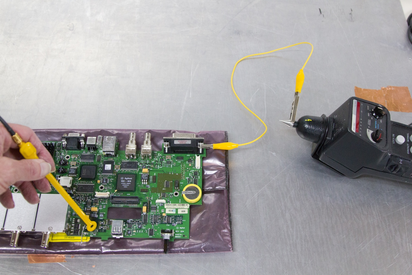 Figure 6. The ESD simulator is adjusted to a safe voltage, such as 500 volts, and connected through the contact discharge tip to the demonstration board under test. The H-field probe is scanned around the board while observing the highest amplitude voltage peaks.
Figure 7 shows a typical ringing pulse from the H-field probe. The ringing is largely due to the inductance of the long clip leads attached to the demo board resonating with the board-to-plane capacitance and is of no consequence, since the important factor is the general amplitude of the pulse.
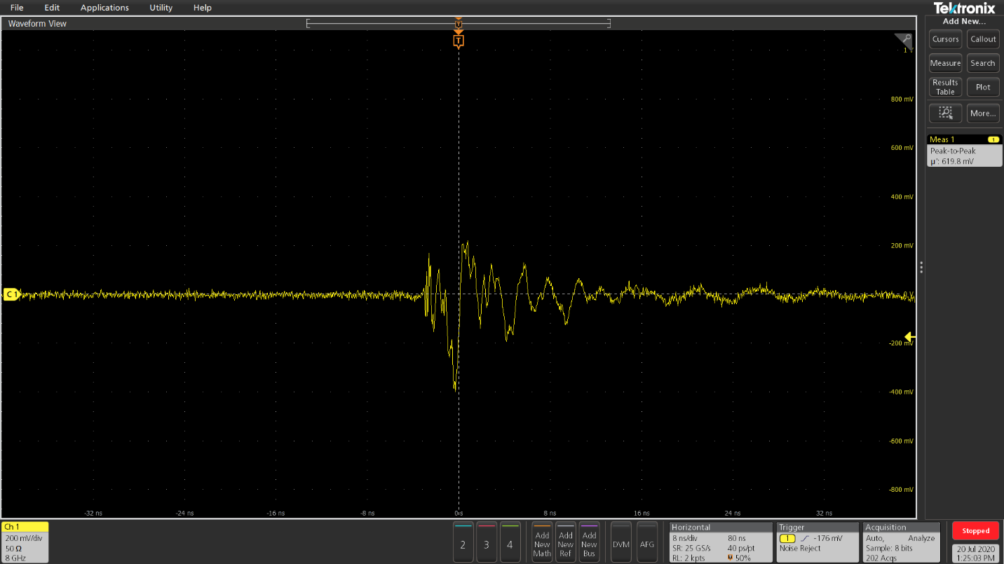 Figure 7. A typical ringing pulse being coupled to the H-field probe while tracing the path of ESD current.
Once the path or paths of dominant ESD current are identified, then mitigations may begin. This usually involves blocking or diverting the ESD current. We want to avoid allowing ESD current through circuit boards. Most line-operated products are connected to earth through the safety wiring, so often it's best to try diverting the ESD current to chassis or the green wire safety, ground through better connector bonding and grounding techniques to chassis.
This diversion path should occur "upstream" from any electronic circuitry, usually right at the I/O and power connectors, or egress points where ESD is tested. For portable devices, the ESD current should be diverted to the digital return plane at the board I/O and power connectors.
Another technique is to introduce blocking impedances, such as ferrite chokes, on any cables that are carrying dominant ESD currents. Also, for digital lines, a combination of series resistance (470 to 1,000 Ohms) and parallel transient protection to the digital return plane or chassis ground works well. This should be located as close as possible to the I/O connectors. All I/O and power connector ground shells should be bonded through short connections to the chassis or to the digital ground return plane. Usually, a combination of blocking and diverting techniques are sufficient to mitigate ESD compliance failures. Of course, it's even better to design these mitigations into the product or system at the start!
ESD is usually tough to troubleshoot without the ability to force a failure. This can be done using any of the simple ESD generators, or better, with an ESD simulator. These can be purchased used or new, but expect to pay $20 to $30k for a new one. A used Keytek MiniZap, or other ESD simulator, would make a good addition to your kit, if you can find one with all the accessories.
Troubleshooting ESD is all about tracing the path of ESD current. This can be easily done by using the HP 457A current tracer probe or better yet, simply using a medium-sized H-field probe and tracing the path using an oscilloscope.
References
- HP 547A current tracer probe
- HP 547A user manual
- Trace ESD current paths with the HP 547A
- Create Your Own EMC Troubleshooting Kit (Volume 1)