Magnitudes and phase delays of the mixed-mode S-parameters are compared in Fig. 27. Again, we can observe good correlation in the insertion losses and transmission phase delays. Though, the model predicts practically no mode transformations due to geometrical symmetry of the structure, but in reality we can observe the modal transformation at around –30 dB. Single-ended and mixed-mode TDRs shown in Fig. 28 reveal possible reasons of the mismatch in the reflection and mode transformation parameters –we can see about 1 Ohm impedance variations along the strips (close to the expectations based on the data provided by manufacturer). We can also see about 3 Ohm difference between the model and measurement at the connector-to-launch interface. That will be further investigated to improve the model. Notice that the connector impedance came out closer to 51.5 Ohm, instead of 50 Ohm claimed by the manufacturer. A model from the manufacturer or based on the connector geometry would not be very helpful in such case (it is usually very close to 50 Ohm). The variations along the traces have a statistical nature and cannot be directly accounted for in the model. It can be done only if the statistical distributions for strip width, dielectric thickness, and possible variations of the dielectric parameters are known. Evaluation of the statistical manufacturing distributions should be done for each manufacturer or provided by the manufacturer. The alternative is to select a more accurate manufacturing process.

Figure 29. 10 cm differential microstrip link in layer BOTTOM – measured and modeled magnitudes of single-ended S-parameters.

Figure 30. 10 cm differential microstrip link in layer BOTTOM – measured and modeled mixed-mode S-parameters magnitude (left plot) and phase delay for diff. and common mode transmission parameters (right plot).

Figure 31. 10 cm differential microstrip link in layer BOTTOM – single-ended (left plot) and mixed-mode (right plot) measured and modeled TDRs.
Results of validation for the 10 cm microstrip link in layer BOTTOM are shown in Fig. 29-31. We can observe good correlation of single-ended transmission, FEXT, and NEXT up to 30 GHz shown in Fig. 29 (though the measured reflection is larger than expected from about 10 to 25 GHz). Similar differential mode reflection mismatch can be observed in Fig. 30. The reason is probably the same as in the case of strip line: the mismatch at the connector-to-launch interface and impedance variation along the traces visible on the TDR plots in Fig. 31. The variations on TDR plots also explain the geometrical un-symmetry of the actual link and non-zero modal transformation parameters as the consequence as shown in Fig. 30. Note that widths and shape of all microstrip traces and solder mask layer parameters were adjusted as identified earlier. Without such adjustments, the measured and modeled impedances are about 3 Ohm off for the single-ended traces and about 6 Ohm off for the differential traces. Amazingly, this difference is within the expected 8% impedance variations (see Fig. 1).
To validate the dielectric and conductor roughness models, we can use the Beatty standard. This is the link with the 2.5 cm wider strip section in the middle as shown in Fig. 32. Measured and modeled magnitudes of S-parameters are shown in Fig. 33. It is difficult to see where the resonances in the reflection are (resonance frequencies can be used to validate the dielectric model [1]). If the loss separation technique did not work, the dielectric will have lower or higher losses. That causes different dispersion in the real part of permittivity and shift of the resonances as the consequence. Unfortunately, the resonances in the reflection parameters are not clean with the presence of the connectors and launches. To eliminate the effect of them, we used a de-embedding procedure based on the test fixture S-parameter extraction from S-parameters measured for two single-ended strip line segments in layer INNER6 and the cross-section model constructed during the material model identification with GMS-parameters in section 6. This de-embedding technique is available in Simbeor software. In this case, the de-embedding is possible only up to 30 GHz due to the launch localization issues (see next section).

Figure 32. De-compositional analysis of structure D2 – Beatty strip standard in layer INNER6.

Figure 33. D2 Beatty strip standard in layer INNER6 – measured and modeled magnitudes of S-parameters for complete link (left plot) and for the structure without connectors and launches (de-embedded).

Figure 34. Beatty strip standard in layer INNER6 – transmission phase delay (left plot) for the complete and de-embedded structures and TDR for the complete link (right plot).
De-embedding is done to the boundaries of the launch discontinuity selectors (see Fig. 32). The de-embedded results are shown in the right plot of Fig. 33 where we see good correlation in the resonance frequencies and insertion loss. Phase delays for the complete and de-embedded modes are compared in Fig. 34 on the left plot. Measured and simulated TDRs of the complete link are shown in Fig. 34 on the right plot. Overall, we can conclude that the dielectric and conductor roughness models are acceptable for the analysis of the strips within some range of widths.
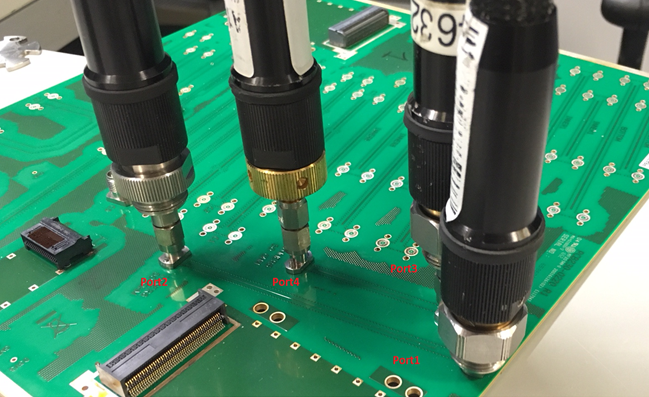
An example of more realistic link with two differential backdrilled vias is the C2 structure shown in Fig. 35. These vias were cross-sectioned and the reality was about 30 um longer stubs (accounted in the analysis). This is very close to the expectations, considering the via performance. Measured and modeled single-ended S-parameters are compared in Fig. 36. There is visible mismatch in the transmission and reflection above 10 GHz and in FEXT and NEXT above 25-30 GHz. Differential transmission and reflection are shown in Fig. 37 on the left plot. The model predicts smaller reflection and transmission from about 10 to 25 GHz. Though, overall the result is acceptable. Differential and common-mode phase delay correlate very well up to about 30 GHz as shown in Fig. 37 on the right plot. Further investigation with TDR shown in Fig. 38 reveals possible source of discrepancies; it is the same mismatch and the connector-to-launch boundary and the impedance variation along the microstrips and strips observed in the other cases. Notice that the strip impedance is more consistent with the expectations (closer to 100 Ohm differential), unlike the microstrip (about 105 Ohm).

Figure 35. C2 link with 2 backdrilled vias and traces in BOTTOM (microstrips) and INNER6 (strips).

Figure 36. C2 link with 2 backdrilled vias – measured and modeled magnitudes of single-ended S-parameters.

Figure 37. C2 link with 2 backdrilled vias – measured and modeled mixed-mode S-parameters magnitude (left plot) and phase delay for diff. and common mode transmission parameters (right plot).
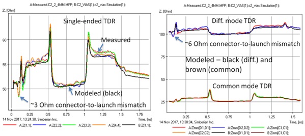
Figure 38. C2 link with 2 backdrilled vias – single-ended (left plot) and mixed-mode (right plot) measured and modeled TDRs.
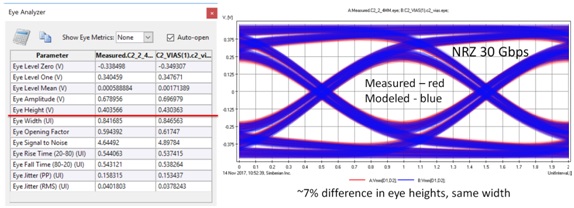
Figure 39. C2 link with 2 backdrilled vias – comparison of measured and modeled eye diagrams for 30 Gbps NRZ signal (no random jitter).
Finally, comparison of the measured and modeled eye diagrams for 30 Gbps NRZ signal without random jitter is shown in Fig. 39. Despite all those discrepancies in the reflection and TDRs, unexpected mode transformations and problems above 30 GHz, the eyes are very close to each other. Only formal analysis reveals about 7% difference in the vertical opening. The horizontal openings are practically the same. The measured vertical eye opening is smaller due to slightly larger insertion loss at about 15 GHz due to larger reflections (or cut of S-parameters below 70 MHz). These reflections are caused by the connector-to-launch mismatch and the manufacturing impedance variations. With small differences in S-parameters up to 30 GHz, one should expect almost identical eyes. On the other hand, when the measured and modeled eyes are visually different, it usually means big differences in the measured and modeled S-parameters and TDRs. This example shows that the eye comparison is the least informative metric. Though, it is practically important to gain the confidence in the approach. Thus, we do it only for some test structures. Comparisons and observations for all other structures on the validation board are provided in the complete report [9]. We can state that the models obtained following the formal procedure have accuracy acceptable up to about 30 GHz, and that is sufficient for the analysis of PCB links for 30 Gbps NRZ signals.
Reality above 30 GHz (complimentary)
Investigation of measured S-parameters above 30 GHz may be the most interesting part of this project. The first peculiarity observed in the measured insertion loss for the straight traces was the resonances around 33 GHz as shown in Fig. 40. The resonances were observed in S-parameters measured with TDNA and all VNAs. It is known that the fiber-weave effect may cause the resonances due to periodic loading of the traces. In this case, we should observe the reflections at the same frequency: periodic changes of the impedance should reflect energy. In this case, we did not observe peaks in the reflection parameters as shown in Fig. 40 on the right plot. So the fiber-weave effect was ruled out. When we looked at the near-end and far-end crosstalk parameters (NEXT and FEXT), and we observed matching peaks as shown in Fig. 41. A de-compositional model of the links with separate models for launches and transmission lines did not predict this coupling. However, the electromagnetic analysis of the launch showed that the energy leaks the launches at the wider gaps between the vias as illustrated in Fig. 42 and Fig. 43 at 33 GHz.

Figure 40. Differential insertion loss (left plot) and reflection loss (right plot) for 3 differential links.

Figure 41. Single ended insertion loss (left bottom plot) and near end crosstalk (NEXT, right top plot) and far end crosstalk (FEXT) for 3 differential links.

Figure 42. Instantaneous power flow density at the microstrip launch at 33 GHz. The electromagnetic field is confined by the closely spaced stitching vias but “leaks” through the wider gap between the vias at the strip side.
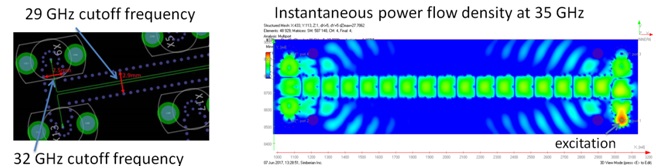
Figure 43. Stitching vias along the traces form waveguides with the cutoff frequencies 29 and 32 GHz. Waves can propagate in such waveguides at any stackup layer as illustrated on the right.
The energy simply leaks into the substrate integrated waveguides (SIW) formed by rows of the stitching vias along the traces, propagates along the waveguide and can be transferred to all other ports in the structure. Every plane pair in this configuration forms the SIW and transmits the waves in addition to the strip or microstrip lines. Pairs with larger distance transmit more energy (wave attenuation is smaller for planes with larger distance). The analysis of this effect requires analysis of the link as a whole; this is time consuming but not necessary. We can simply predict such behavior with the analysis of the launch and evaluation of the cutoff frequency for the SIW.
Note that the strip lines are waveguides with two reference planes and the equipotentiality must be always enforced with stitching vias to have predictable behavior at the microwave frequencies. To extend the frequency range of the interconnects up to 40-50 GHz, here are some recommendations:
- Launch return vias should be closer to the signal via: the distance between the vias can be used to evaluate the upper localization frequency
- Gaps between the stitching vias on the strip side should be as small as possible
- Stitching vias along the strips should be closer to the strip. Cutoff frequency of SIW can be used to compute this distance and the effect of the vias should be evaluated to avoid the periodic loading
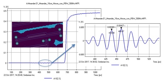
Figure 44. Ripples in the TDT response of the meandering strip line in layer INNER6.

Figure 45. Instantaneous power flow density in the meandering strip line (left) – power flows along the traces and along the SIW formed by stitching vias (right).
Another peculiarity observed in the measurements was the ripples in the TDT response for the meandering strip line as shown in Fig. 44. It looks like a non-causality at the first glance, but it is actually the multipath propagation phenomenon caused by the “leaks” from the launches and energy transmission through the SIW formed by the solid planes and rows of stitching vias as illustrated in Fig. 45. The power propagates along the strips and also along the SIW, as visible on the left and right plots in Fig. 45.
Finally, coupling between the ports in two different strip line links in layer INNER6 was measured as shown in Fig. 46 Ideally, the coupling should be zero, but in reality it is below -70 dB up to 25-27 GHz and grows at higher frequencies. To reduce such coupling, more stitching vias should be placed between the structures and all over the board. Note that this is applicable not only for the strip reference planes, but to all parallel plane structures; the energy can be transferred between any pair of planes.

Figure 46. Measurement setup to evaluate coupling between ports in two different strip links (left) and coupling parameters (right plot).
Conclusion
A “sink or swim” validation process [3] has been successfully used in this “practical” analysis-to-measurement validation project. So far, the acceptable analysis-to-measurement correlation has been reached up to 30 GHz on most of the structures. Technically, this is sufficient for the reliable analysis of 28-32 Gbps links.
Design of launches and reference plane stitching localization degraded the correlation above 30 GHz. These effects are difficult to simulate or to predict, even for simple validation boards. Also, the accurate prediction of PCB behavior at the millimeter bandwidth up to 40-50 GHz with the typical trace width and low-cost manufacturing process with large geometry variations is very ambitious and may not even be possible. It would be practically impossible to include all of those variations in the analysis because of a lack of the statistical distributions of the board geometry and material parameters. In addition to the statistical manufacturing variations, considerable differences in the microstrip trace geometry have been discovered during cross-sectioning. The bottom line: do not expect excellent analysis-to-measurement correlation with the low-cost manufacturing processes and without cross-sectioning of the board! To extend the predictability up to 40-50 GHz, manufacturing tolerances should be substantially reduced, or trace widths increased and more homogeneous dielectrics used (or all of the above).
The specificity of the signal integrity problems also dictates very strict requirements for the measurement equipment: accuracy at low and high frequencies is equally important. The reality is that not all measurement equipment satisfies such requirements. Anyone with plans to purchase the equipment (or EDA tools) should try it first without regards to the vendor profile and have software or an expert in the team to evaluate S-parameters quality and validity. Validation boards are excellent tools to do that. The measurement and EDA tools may be very expensive and not as accurate as claimed by the vendors. The selection of the measurement equipment and components caused substantial delay in this project. Here are some other practical observations:
- Identified dielectric parameters are very close to the vendor specs
- Conductor roughness is the major contributor to the signal degradation - analysis without proper conductor roughness models is useless
- The Causal Huray-Bracken conductor roughness model provided good correlation in the losses and in the TDR impedance
- Cross-sectioning revealed that the strip traces are very close to the adjusted trace geometry provided by manufacturer, however, the microstrip cross-sections are very different
- Measurements should be planned in advance to have all matching parts (cables/connectors)
- Layout needs careful inspection before and after the manufacturing
- Naming for stackup and nets should be consistent through the whole design/manufacturing cycle
- To simplify comparisons, port numeration should be consistent in models and measurements
This is an ongoing project, and we keep investigating obtained data in preparation for the next validation board. We expect it will be actually predictable up to 40 GHz!
This article is an edited version of a DesignCon 2018 Best Paper Award winner.
Download the full paper here
Acknowledgments
The authors gratefully acknowledge Ingvar Karlsson, Kunia Aihara, Davood Khoda, Kenneth Jonsson, Matti Nuutinen for valuable help during this lengthy project.
References
- Y. Shlepnev, A. Neves, T. Dagostino, S. McMorrow, Measurement-Assisted Electromagnetic Extraction of Interconnect Parameters on Low-Cost FR-4 boards for 6-20 Gb/sec Applications, DesignCon2009.
- D. Dunham, J. Lee, S. McMorrow, Y. Shlepnev, 2.4mm Design/Optimization with 50 GHz Material Characterization, DesignCon2011.
- Y. Shlepnev, Sink or swim at 28 Gbps, The PCB Design Magazine, October 2014, p. 12-23.
- W. Beyene, Y.-C. Hahm, J. Ren, D. Secker, D. Mullen, Y. Shlepnev, Lessons learned: How to Make Predictable PCB Interconnects for Data Rates of 50 Gbps and Beyond, DesignCon2014.
- Y. Shlepnev, Broadband material model identification with GMS-parameters, Proc. of 2015 IEEE 24st Conf. on Electrical Performance of Electronic Packaging and Systems (EPEPS'2015), San Jose, 2015.
- Y. Shlepnev, Y. Choi, C. Cheng, Y. Damgaci, Drawbacks and Possible Improvements of Short Pulse Propagation Technique, Proc. of 2016 IEEE 25st Conf. on Electrical Performance of Electronic Packaging and Systems (EPEPS'2016), pp. 141-143, October 23-26, 2016, San Diego, CA.
- J. Martens, B. Buxton Signal Integrity: Frequency Range Matters!, Anritsu app note
- Sensitivity of PCB Material Identification with GMS-Parameters to Variations in Test Fixtures – Simberian app note #2010_03.
- M. Marin, Y. Shlepnev, 40 GHz PCB Interconnect Validation: Expectations vs Reality – complete report and solutions, available on request.
Author(s) Biography
Marko Marin is electronics design engineer with Infinera Metro HW in Stockholm Sweden, where he focuses on high speed serial design, SI/PI modeling and characterization using EDA tools and measurement equipment. Prior joining Infinera in 2016, he was at Ericsson Digital HW, working as a signal integrity engineer. Marko holds MSc in electrical engineering from Royal Institute of Technology, Stockholm, Sweden
Yuriy Shlepnev is President and Founder of Simberian Inc., where he develops Simbeor electromagnetic signal integrity software. He received a M.S. degree in radio engineering from Novosibirsk State Technical University in 1983, and the Ph.D. degree in computational electromagnetics from Siberian State University of Telecommunications and Informatics in 1990. He was principal developer of electromagnetic simulator for Eagleware Corporation and the leading developer of electromagnetic software for simulation of signal and power distribution networks at Mentor Graphics. The results of his research are published in multiple papers and conference proceedings.