
We worry about via stubs in high-speed designs because they cause unwanted resonant frequency nulls which appear in the insertion loss plot (IL) of the channel. But are all via stubs bad? Well, as with most answers relating to signal integrity, “It depends.”
If one of these frequency nulls happen to line up at or near the Nyquist frequency of the bit- rate (i.e. 1/2 of the bit-rate), the received eye will be devastated, resulting in a high bit-error-ratio (BER), or even link failure.
Figure 1 shows simulation results of two backplane channels. On the left are measured SDD21 insertion loss and eye diagram of a 10 GB/s, non-return-to-zero (NRZ) signal, with short through vias and long stubs ~ 270 mils. On the right, shows measured SDD21 IL and eye diagram of a channel with long through vias and shorter stubs ~ 65 mils.
Keysight EEsof EDA Advanced Design Software (ADS) S-parameter pallet was used to plot the measured SDD21 IL. The channel simulator pallet was used to simulate the eyes and BER contours.
Because the ¼ -wave resonant null occurs at a frequency ~ 4. 4 GHz, this is near the Nyquist frequency for 10 GB/s. As can be seen, the eye is totally closed, for the long stub case. But when the shorter stub case is simulated, the eye is open. The contour plot shows plenty of margin for a BER of 10E-12.
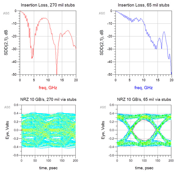
Figure 1. Simulation results at 10GB/s of a backplane channel with ~ 270 mils via stubs (left) vs a channel with ~ 65 mils via stubs (right). BER contour is 1E-12. Simulated with Keysight EEsof EDA ADS software.
So how does a via stub cause ¼ -wave resonance? This question can be explained with the aid of Figure 2. Starting on the left, we see a via with two sections. The through (thru) part is the top portion connecting a device pin to an inner layer trace of a printed circuit board (PCB). The stub portion is the lower portion and is an open circuit.
On the right let’s assume a sinusoidal signal is injected into the pin at the top of the via and travels along the thru portion until it reaches the junction of the internal trace and stub. At that point, the signal splits. Some of it travels along the trace, and the rest continues down the stub. Once it reaches the bottom, it reflects back up. When it reaches the trace junction, it splits again with a portion traveling along the trace and the rest back to the source.
If f is the frequency of a sine wave, and the time delay (TD) through the stub portion equals a ¼ -wavelength, then when it reflects at the bottom and reaches the junction again, it will be delayed by ½ a cycle. At this point it is 180 degrees out of phase, and cancels most of the original signal.
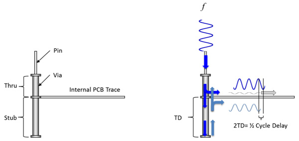
Figure 2. Illustration of a ¼ -wave resonance of a stub. If f = frequency where TD = ¼ wavelength, then when 2TD = ½ cycle minimum signal received.
Resonance nulls occurs at the fundamental frequency fo and at every odd harmonic. If you know the length of the stub (in inches) and the effective dielectric constant (Dkeff), surrounding the via hole structure, the resonant frequency can be predicted by:
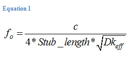
Where: fo is the ¼ -wave resonant frequency (GHz); c is the speed of light (~11.8 in/ns); Stub_length is inches.
You will find that Dkeff is not the same as the bulk Dk published in laminate manufacturers’ data sheets. It is typically higher. A higher Dkeff increases phase delay through the via resulting in a lower resonant frequency.
One reason is excess capacitance from the via pads as well as the via barrel’s proximity to the clearance hole openings (also known as anti-pads) in plane layers. The other is because of the anisotropic nature of the laminate material.
For the example in Figure 1, the ¼ -wave resonant frequency of the long via stub is ~ 4.4 GHz. With a stub length of ~ 270 mils, this gives a Dkeff of 6.16, which is considerably higher than the published bulk Dk of 3.65. When you model a via in an electro-magnetic (EM) 3D field solver, it automatically accounts for the excess capacitance, but you will still need to compensate for the anisotropic nature of the dielectric.
A material is anisotropic when there are different values for parallel (x-y) vs perpendicular (z) measured values for dielectric constant. Dielectric constant and loss tangent, as published in manufacturers’ data sheets, report perpendicular measured values.
In a paper by P.I. Dankov, “Two-Resonator Method for Characterization of Dielectric Substrate Anisotropy”, he disclosed results of a study on dielectric anisotropy of common fiberglass reinforced substrates used in radio-frequency (RF) designs. For 0.2 mm to 0.3 mm thick substrates, he found a wide variation in anisotropy of samples he tested.
For example, materials with low anisotropic effects between 5% - 15% were non-fiberglass reinforced polytetrafluoroethylene (PTFE) laminates, like Rogers RO4003, while high anisotropic materials between 15% - 25% tended to be fiberglass reinforced laminates, like FR4 type laminates. Unfortunately anisotropic numbers are not available from laminate supplier’s data sheets.
This is consistent with an IEEE paper I coauthored with Yazi Cao and Eric Bogatin titled, “Differential Via Modeling Methodology”. In that study we found that Dkxy needed to be 18% higher to correlate simulation to measured data.
For differentially driven vias with round anti-pads and plane layers evenly distributed throughout the entire stackup, Dkeff can be roughly estimated by:
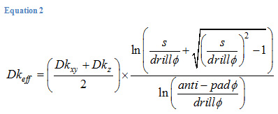
Where: Dkxy is the dielectric constant adjusted for anisotropy; Dkz is the bulk dielectric constant from data sheets; s is via-via spacing; drillØ is drill diameter; anti-padØ is anti-pad diameter.
The effects of via stubs can be mitigated by: using blind or buried vias; back-drilling; or by using thru vias only (i.e. from top layer to bottom layer). Practically, the shortest stub that can be achieved by back-drilling is on the order of 5 to 10 mils.
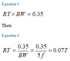
As a rule of thumb, we usually strive to have an interconnect bandwidth (BW) to be five times the Nyquist frequency of the bit-rate. This follows many oscilloscope manufacturers’ specifications for risetime bandwidth product equal to 0.35.
Five times Nyquist represents the 5th harmonic sinusoidal component of a Fourier series making up an ideal square wave shown Figure 3. An interconnect BW up to the 5th harmonic preserves the integrity of risetimes down to 7% of the period of the fundamental frequency.
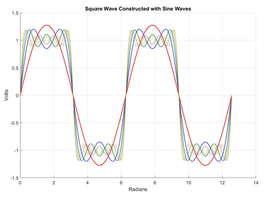
Figure 3. Construction of an ideal square wave from odd harmonics of the fundamental frequency.
If the risetime (RT) bandwidth (BW) product to the 5th harmonic of the fundamental frequency is defined as:
So for example, a 10 GB/s data signal, with a Nyquist frequency (f) of 5 GHz, needs a BW of 25 GHz, to preserve any RT down to 7% of the Nyquist frequency period (T), or 14 ps.
Since a ¼-wave resonant null behaves somewhat like a notch filter, depending on the high-frequency roll-off due to Q-factor, frequencies near resonance will be attenuated. For that reason a good rule of thumb to follow is making sure the first null should occur at the 7th harmonic, or higher, of the Nyquist frequency to maintain the integrity of the 5th harmonic frequency component.
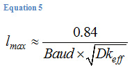
With this in mind, for a given baud-rate (Baud) in GBd/s, the maximum stub length (lmax), in inches can be estimated by:
For NRZ signaling, the baud-rate is equal to the bit rate. But for PAM-4 signaling, which has 2 symbols per bit time, the baud-rate is ½ of that. Thus a 56 GB/s PAM-4 signal has a baud-rate of 28 GBd/s, and the Nyquist frequency is 14 GHz, which happens to be the same as 28 GB/s NRZ signalling.
Figure 4 presents a chart of maximum stub length vs baud-rate based on Equation 5, using a Dkeff = 6.16 (blue) vs 3.65 (red). It shows us the higher the baud-rate, the more the stub length becomes an issue, especially past 10 GBd/s. We also get a feel for the sensitivity of stub length to Dkeff . Even though there is ~ 70% difference in Dkeff, there is only ~ 30% delta in stub lengths for the same baud-rate. This means that even if we use the bulk Dk published in data sheets, we are probably not dead in the water.
If the respective stub length is greater than this, it does not mean there is a show stopper. Depending on how much longer means the eye opening at the receiver will be degraded and we lose margin. We see this by the example in Figure 1. Even though the stub lengths in the channel were almost double the value at 10 GBd/s from the chart, there is still plenty of eye opening.
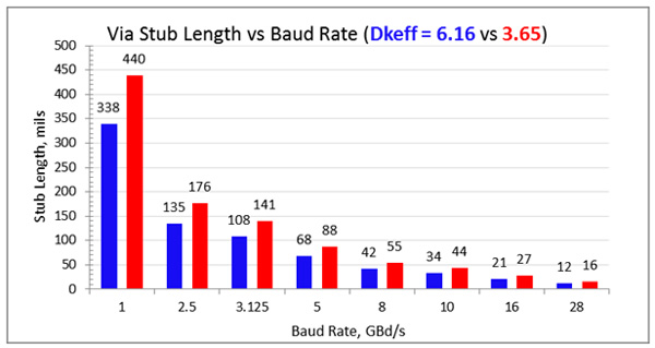
Figure 4. Chart showing estimated maximum stub length vs baud-rate with Dkeff of 6.16 (red) vs 3.65 (blue) based on Equation 5.
To further explore design space and test out the rule of thumb, a circuit model was built using Keysight ADS with the ability to vary the via stub lengths. Referring to the chart, at 28 GBd/s, the maximum stub length should be 12 mils, assuming a Dkeff of 6.16. Figure 5 shows simulation results for NRZ signalling. As can be seen, there was a difference of only 17 mV in eye height (1.5%), and no extra jitter for 12 mil stubs compared to 5 mil stubs.
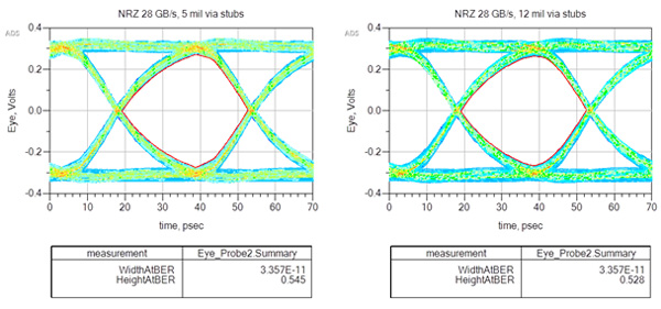
Figure 5. Eye diagrams comparison with BER at 10E-12 for stub lengths of 5 mils vs 12 mils. Modeled and simulated with Keysight ADS.
But if we use the exact same channel model, and use the generic PAM-4 IBIS AMI model from Keysight Technologies, we can see the results plotted in Figure 6. On the left are the eye openings with 5 mil stubs and the right with 12 mil stubs. In this case, there was an average reduction of ~7 mV (6%) in eye heights, and 0.24 ps (2%) in eye widths at BER 10E-12 across all three eyes.
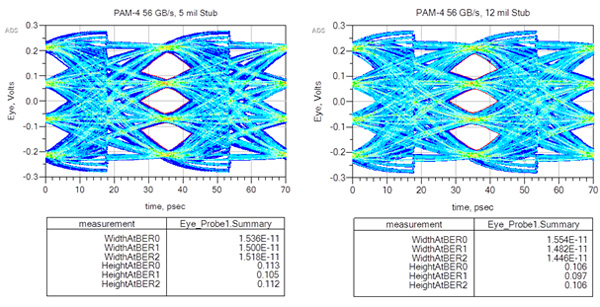
Figure 6. PAM-4, 28 GBd/s (56 GB/s) eye height and width comparison at BER of 10E-12 for 5 mil vs 12 mil stub lengths.
Because PAM-4 signalling has three smaller eyes, that are one-third the size of an NRZ eye for the same amplitude, it is more sensitive to channel impairments. From the above examples, we can see NRZ had only 1.5% reduction in eye height compared to 6% for PAM-4. Similarly there was no increase in jitter for NRZ compared to 2% increase for PAM-4 when stub lengths changed from 5 mils to 12 mils.
What this says is maintaining a BW to 5 times Nyquist rule of thumb, when estimating via stub lengths, is quite conservative for NRZ signalling. There is almost the same BW as the channel with 5 mil stub, which was the original objective. But because PAM-4 is more sensitive to impairments, it shows there is less margin.
In summary then, rules of thumb and related equations are a good way to reinforce your intuitions. They help you know what to expect before you take any measurements or perform any simulations. They can even help you in forensic analysis when things aren’t working in the lab. And, as Eric Bogatin likes to say, “sometimes an OK answer NOW! is better than a good answer late”. But they should never be used to sign off on any high-speed design.
Because every system will have different impairments affecting BER, the only way to know how much margin you have is by modeling the via with a 3-D EM field solver, based on the actual stackup and simulating the entire channel complete with crosstalk, if margins are tight. This is even more critical for data rates above 10 GBd/s.
So to answer the original question, “are all via stubs bad”? Well, the answer is it still depends. For NRZ signalling, there is more leeway than for PAM-4. But we now have a practical way to quickly quantify the answer if we know the stub length, baud-rate and delay through the via.