
Devices mounted to your PC board, such as DC-DC converters, video, and processor/memory, can create enough self-generated EMI to reduce the receive sensitivity of wireless or cellular receivers. This is a real issue for cellular LTE (700 to 850 MHz) bands, because the coupled EMI affects the total isotropic sensitivity (TIS) of the receiver downlink band. Cellular providers require a certain receive sensitivity before they’ll allow a device on their system. I’ve seen some self-generated EMI extend all the way through the GPS and other GNSS systems to the point where they’ll loose lock.
Besides a perfect PC board layout and stack-up, the use of local shields is usually mandatory to prevent external E- and H-fields from coupling through the PC board or directly into antennas. Local board shields need to have multiple connection points to the ground return plane of the board for best H-field shielding (the most common issue).
When considering shielding effectiveness, a general rule of thumb is that any slots in the shield should be no longer than 1/20th of a wavelength at the highest frequency of concern, which will provide about 20 dB of shielding effectiveness. The highest critical receive frequency would be the GPS band at around 1575 MHz, so 1 cm spacing for the grounding pins or tabs on the local shield should be sufficient. The Wi-Fi bands (2.5 and 5 GHz) do not nearly have such a sensitivity issue to self-generated EMI.
However, having said that, my experience with cellular LTE (700 to 850 MHz) modules is that ANY self-generated emissions from the board should have a continuous soldered connection around the perimeter of the shield for lowest risk of EMI coupling.
Local Shield Examples
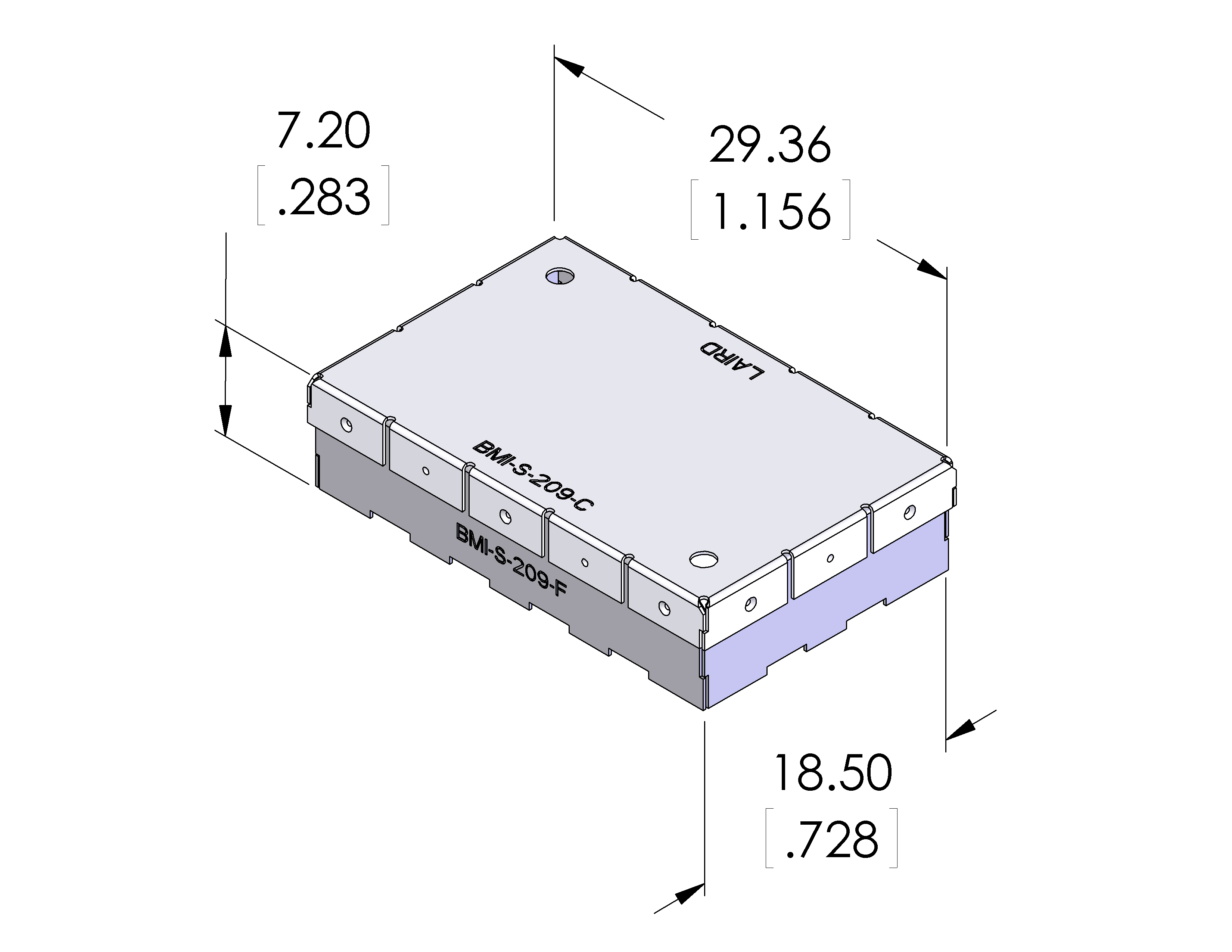
Figure 1 is an example of a good shield for H-fields, as the solder tabs are closer together. Some local shields even have continuous soldering around the perimeter for critical RF or military applications.

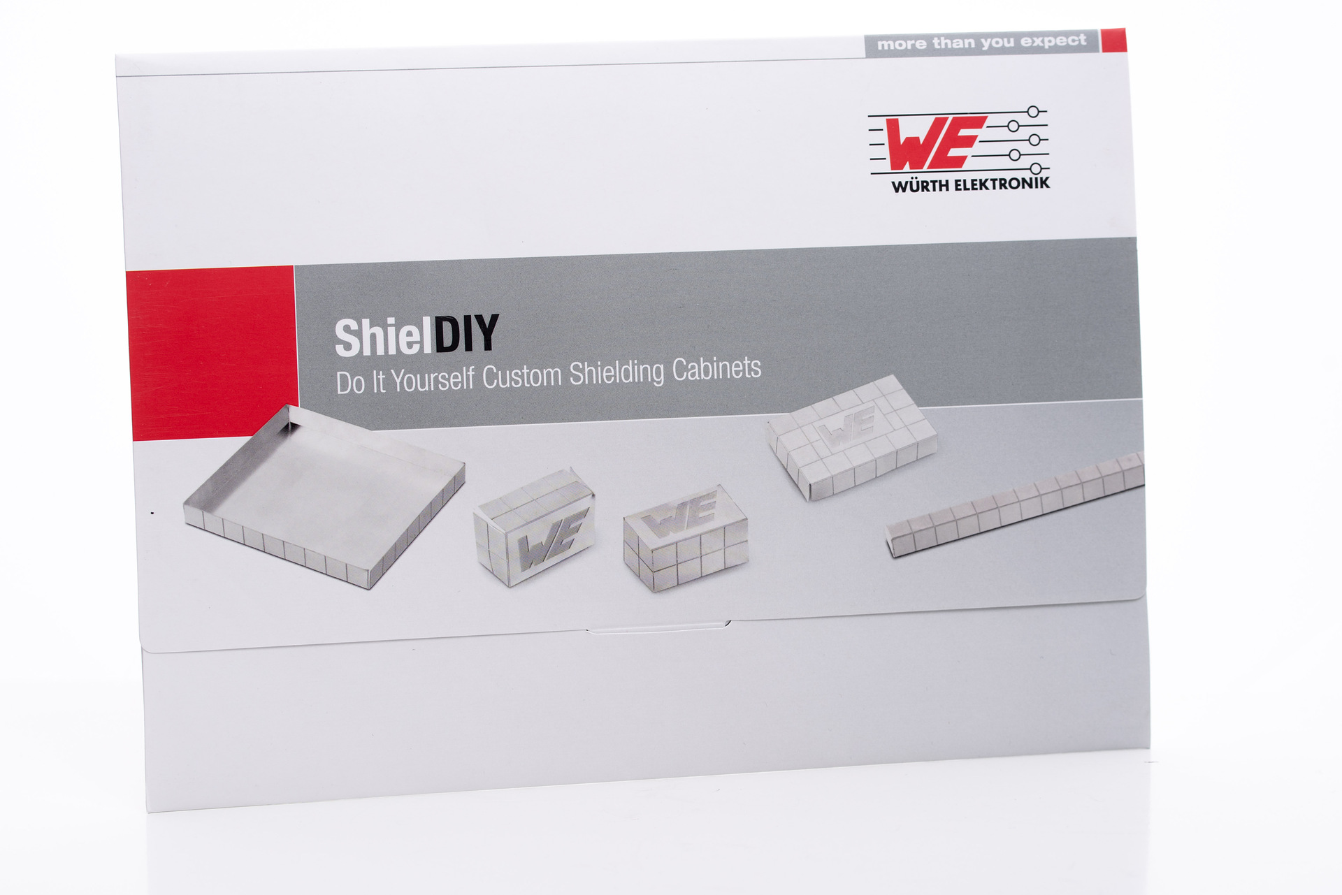
Besides the conventional customizable shields (Figure 2), Würth Elektronik also offers a “DIY Kit” as shown in Figure 3. These shield templates may be folded in many different shapes and sizes.

The advantage of the XGR system (Figure 4) is that it is custom-formed and easily attached during the surface-mount process.
Penetrating Shields with Traces
For best results, any trace that penetrates through a shield boundary should be filtered appropriately. This is commonly done in military or aerospace applications.
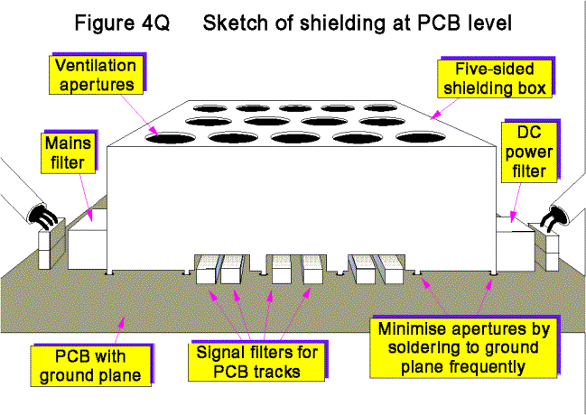
Figure 5 shows an example of typical mounting details for a local shield over a power supply as well as filters for traces penetrating the shield boundary. Mains and output filters should be located close to the shield.
Shield Boundary
The shield boundary is merely the boundary around critical circuitry, such as DC-DC converters, that will accommodate connections to a local board shield. See the above figure for an example. This can be continuous or simply closely-spaced solderable points where the local shield may be soldered onto the board. Shown in Figure 6 is a continuous solderable trace (or boundary) with multiple vias connected to the ground return plane.

Another example showing the shield boundary and solder points over a processor and memory is the two smaller shield locations covering DC-DC converters (Figure 7).

With bonding pins (or tabs) far apart (Figure 8), the shield will be effective for E-fields (DC-DC converter switch node, for example), but not H-fields. Most dominant fields on a board will be H-fields (high frequency current through traces).
Partitioning Circuit Functions
One concept of great importance for critical wireless applications is partitioning of circuit functions (Figure 9). By partitioning noisy circuitry (DC-DC converters and processor/memory) together and away from sensitive wireless modules, it makes it easier to apply local shields.
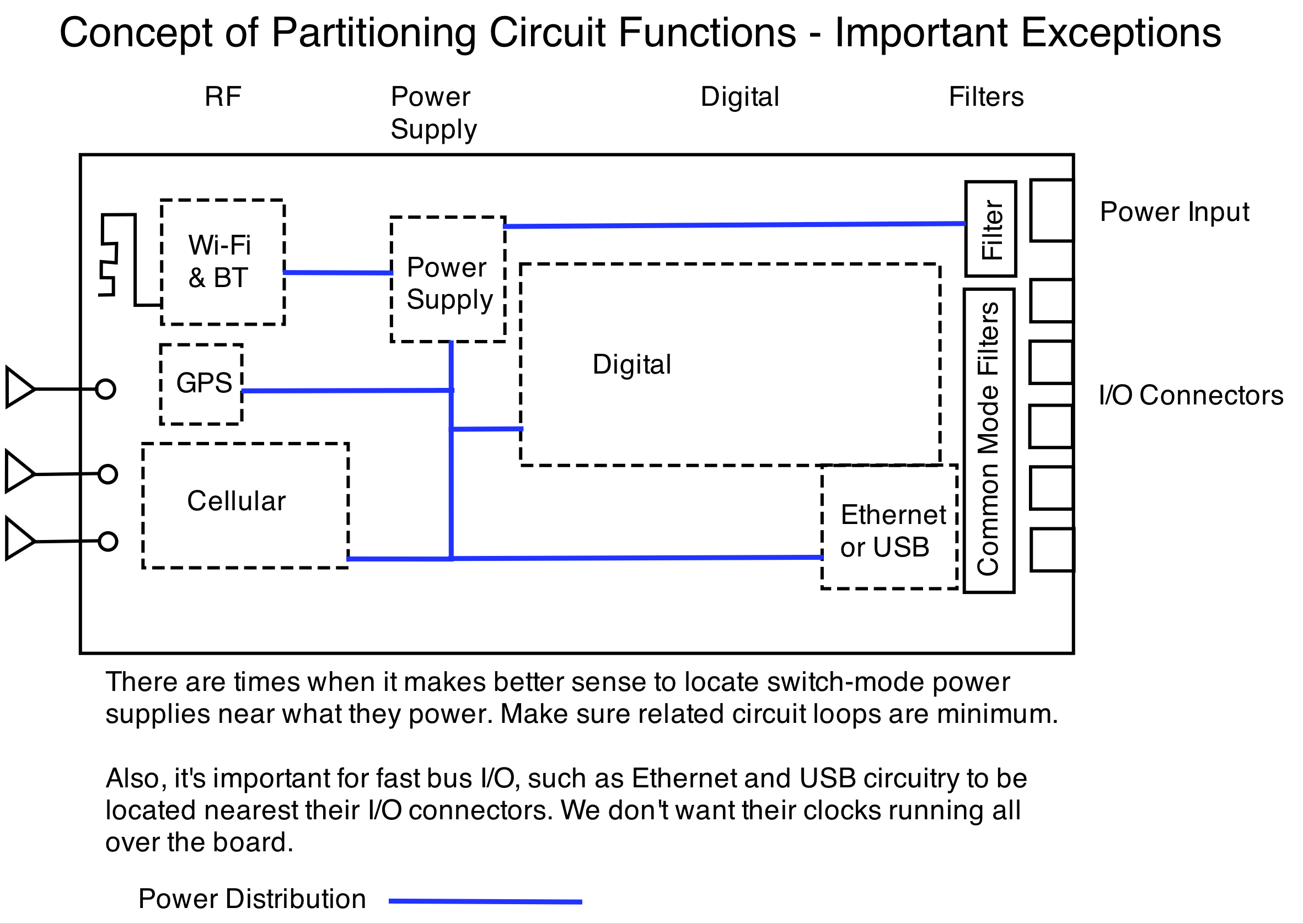
Because return currents tend to flow directly underneath signal and power traces at frequencies above 100 kHz, we can use this self-isolation property to separate noisy circuits from quiet circuits through the use of partitioning of major circuit functions, and yet use a solid return plane for the board.
For example, by keeping the digital processing separate from the RF sections, we help reduce the associated noise return currents from coupling to sensitive receivers.
While I indicate power distribution by a blue line, you could also use a solid power plane for the primary 3.3 V digital source and can optionally run it across the entire board, depending on the power requirements of the system. It should certainly be a solid power plane under all digital processing circuitry and using plenty of decoupling capacitors to an adjacent return plane.
It’s not always realistic to separate circuit functions in the simplistic model shown, but it is very important to isolate known noise sources from wireless and cellular modules. Grouping all the wireless circuitry together and away from noisy digital processing and power converters is key goal. And while I show the power conversion as a separate block, it is often located closer to the power input connector or also distributed closer to the load it’s powering. I’d still keep all DC-DC converters far away from wireless modules.
Summary
I find from experience, that for most critical wireless applications – especially ones that include cellular LTE modules in the 700 to 850 MHz bands), important energy sources that usually require local shields include DC-DC converters, processors and memory, Ethernet, USB, bus transceivers, FPGAs, or other custom ICs – planning in advance to install local shields may prevent an additional board spin. It is also important to have solder points to the digital return plane for troubleshooting purposes. If you find shields aren’t required, then you won’t have lost any time or money.
There are many vendors of local shields. Here are a few I recommend.
Resources
- Wyatt, Platform Interference (EDN).
- Wyatt, Debugging EMI Issues for Wireless and IoT Products Using an Oscilloscope (video).
- Wyatt, EMI Q&A: Reduce on-board DC-DC converter EMI for wireless/IoT devices (EDN).
- Wyatt, Characterize DC-DC converter EMI with near-field probes (EDN).
- Wyatt, Workbench Troubleshooting EMC Emissions (Volume 2), Chapter 7 (Troubleshooting Wireless Interference).