


The question on whether the ground return plane should be cut away under the switch node or inductor of DC-DC converters has been an ongoing debate.
The argument for an adjacent solid plane under all converter circuitry has been to contain the electromagnetic fields in the dielectric space between the circuit traces and return plane; that this would prevent the spread of EMI around the board.
Others argue the capacitive coupling between circuit traces and return plane should be cut away to minimize the capacitive coupling due to large dV/dt swings of the converter switch node with corresponding contamination of the return plane with EMI. In addition, there is concern for induced eddy currents on any solid plane below the inductor. Although, any eddy currents generated by the inductor tend to self-cancel and reduce the overall field level from the inductor (depending on the type and mounting orientation).
My colleague, Steve Sandler, decided to investigate the issue by designing four identical buck converter circuits (Figure 1) with component layout (Figure 2), built on a two-layer stack-up (Figure 3). The experiment was designed to compare (1) a solid return plane with, (2) a cutout at the switch node pad, (3) a cutout under the switch inductor, and (4) a cutout under both the switch node and inductor. See Figure 4 for the four return plane designs.
Converter Design
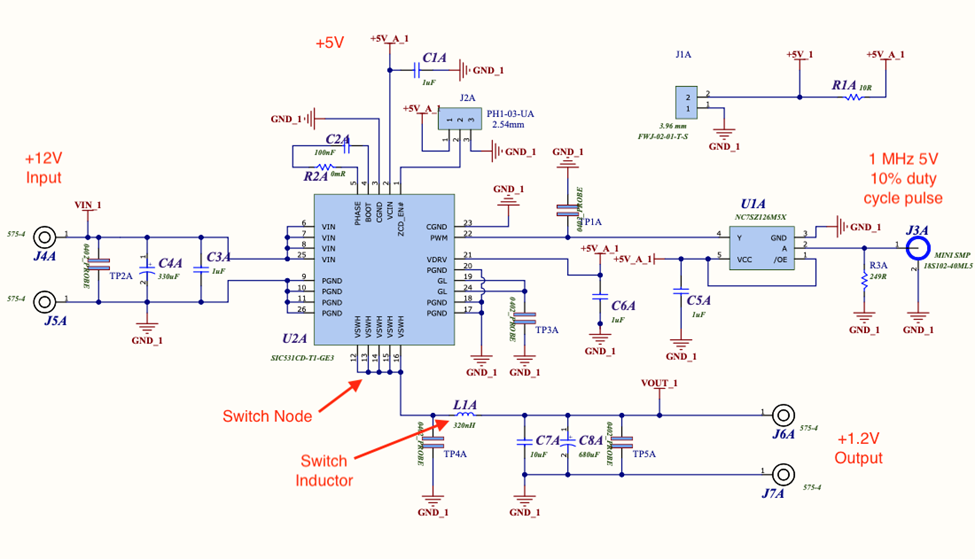 Figure 1. The schematic diagram for all four converters.
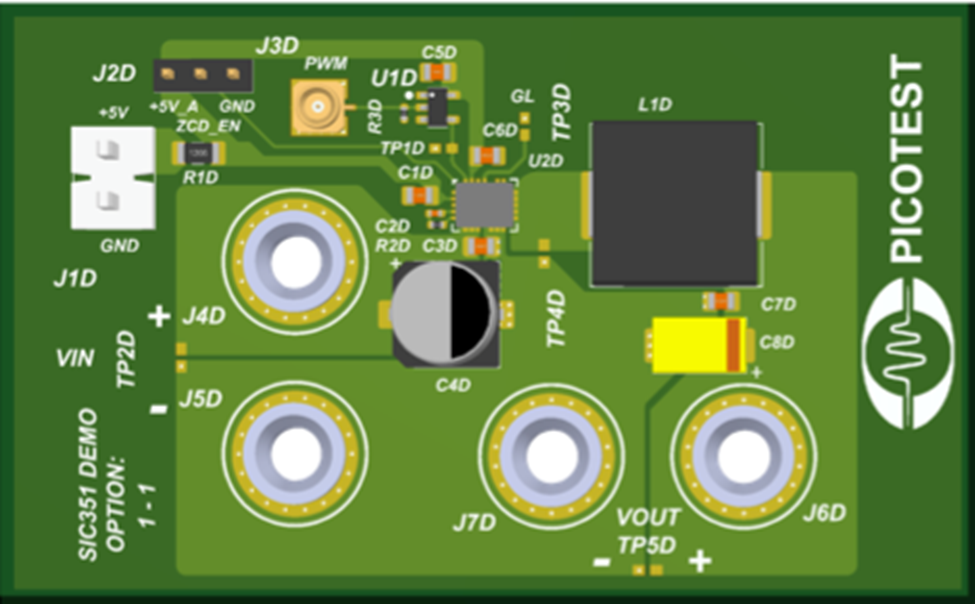
Figure 2. A graphic diagram of the component layout.
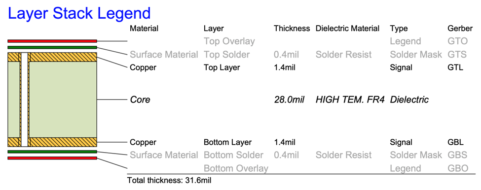
Figure 3. The stack-up design used. The bottom layer was solid, except for the voids added.
The four boards were labeled as (see Figure 4):
 Figure 4. The four converter boards showing the return plane (bottom layer) cutouts for the four configurations.
EMC Testing
The two biggest questions in my mind were how the performance of the four boards compared for radiated and conducted emissions.
Conducted Emissions
- Conventional 5µH DC LISN – This is the conventional method employed per CISPR 15 for automotive modules. The spectrum analyzer was connected to the LISN. Various frequency ranges were measured with markers positioned at sample frequency peaks with amplitudes measured.
- Current Probe on Vin Cable – The RF current probe was connected directly to a spectrum analyzer and markers were positioned at sample peaks and amplitudes measured.
- LISN Mate Testing – Using the LISN Mate with a pair of conventional 5µH DC LISNs allows splitting the differential mode and common mode currents and measuring each independently on sample frequency peaks.
Radiated Emissions
Test Equipment Used:
- Tekbox Digital Solutions 5 µH LISN, model TBOH01 (x2)
- Siglent Technologies spectrum analyzer, model SSA 3032X (9 kHz to 3.2 GHz)
- Rigol Technologies spectrum analyzer, model DSA815TG (9 kHz to 1.5 GHz) – for Y.I.C EMScanner
- Siglent Technologies function/arbitrary waveform generator, model SDG 1062X
- Siglent Technologies dual power supply, model SPD3303C
- Rigol Technologies active load, model DL3021
- Tekbox Digital Solutions LISN Mate, model TBLM01
- Fischer Custom Communications RF current probe, model F-33-1
- Y.I.C. Technologies, EMScanner, 150 kHz to 8 GHz, model EMS8000.
Strips of aluminum foil were taped to the work bench to simulate a conductive ground plane. The LISNs were bonded to this plane with adhesive copper tape. The board under test was placed on an insulated spacer. The general test setup is shown in Figure 5.
Figure 5. The general test setup for the conducted emission measurements. In this case, the LISN Mate configuration is shown.
The four test setup diagrams are shown in Figures 6, 7, 8 and 9. A 1A load was applied to each board.
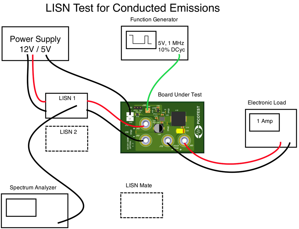
Figure 6. The test setup for the conventional LISN test of conducted emissions. This was the first test performed.
 Figure 7. The test of conducted emissions using a conventional RF current probe to measure the level of common mode currents in the power input wires.
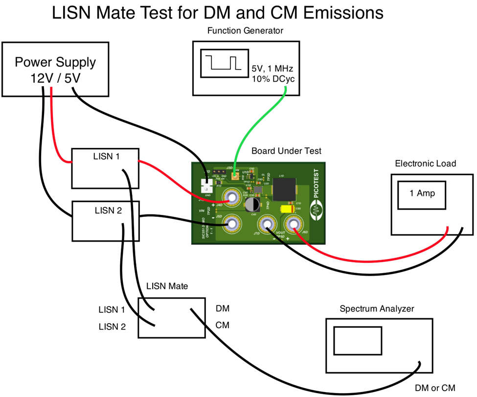
Figure 8. The test setup using the LISN Mate to differentiate between differential mode and common mode currents.
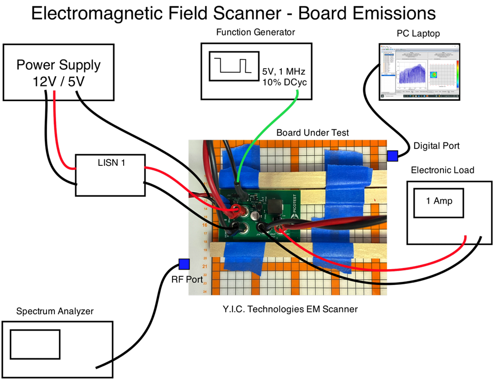
Figure 9. The test setup using the Y.I.C. Technologies electromagnetic field scanner to map out the H-fields emanating from the PC board.
Figure 10 shows the overall test setup for the Y.I.C. Technologies electromagnetic field scanner. It is comprised of an array of 1218 tiny H-field loops throughout the gridded area of the scanner. A PC board was placed over the grid and defining the area to capture results in a maximized plot of harmonic emissions, as well as a “heat map” of near field H-fields present around the board.
A wooden jig was taped down to ensure correct positioning of each board measured. The antenna array grid under the PC board, as well as the lower and upper frequency limits, were defined in software.
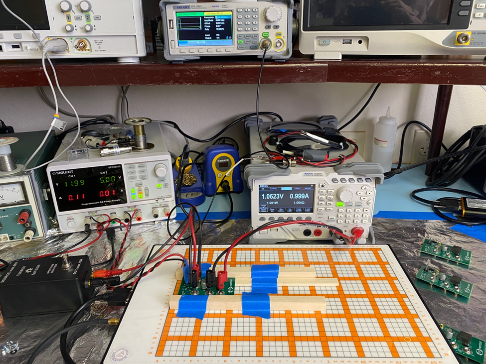
Figure 10. The overall test setup using an electromagnetic field scanner from Y.I.C Technologies to map the fields surrounding the board. A jig of wood was used to ensure board to board positioning accuracy.
Test Procedure – Conducted Emissions
The test procedure was developed as I explored the best way to measure the data. The differences were typically between 0.5 and 4 dB, so it was refined as I proceeded through the four types of measurements.
Because the harmonic amplitude differences from board to board were very small, I eventually placed markers (four maximum for the Siglent spectrum analyzer) on random peaks spread along the measured spectrum and displayed a “marker table,” which showed the amplitudes of each peak.
Each of the four boards was measured using the same four markers and the data compared and plotted. This method was used for each board and separate scans were done from 150 kHz to 30 MHz and 30 to 500 MHz. Confirmation testing was done later between 150 kHz to 100 MHz. Figures 11, 12 and 13 show typical spectral responses from the various tests.
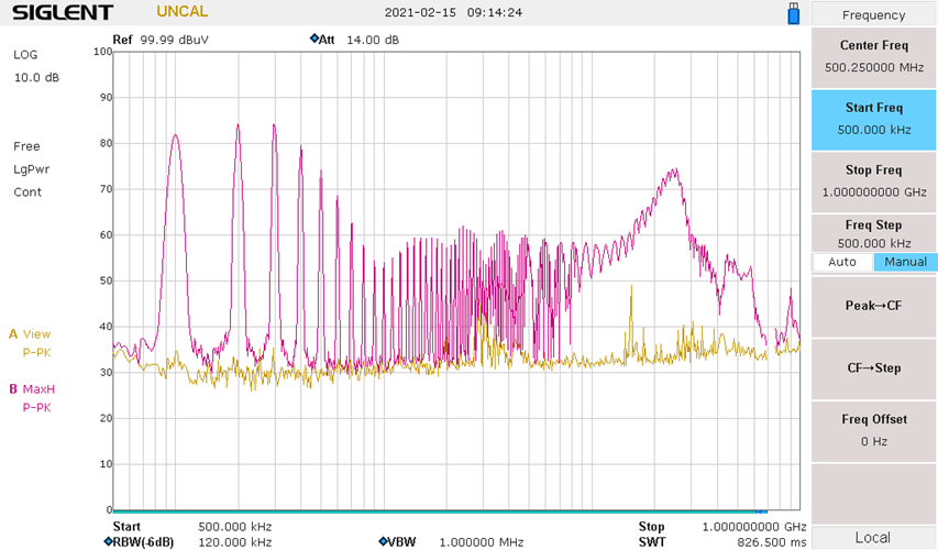 Figure 11. A typical conducted emission spectrum (500 kHz to 1 GHz) using the conventional LISN. The peak at about 230 MHz was due to a strong ringing on the switch node. The yellow trace is the system noise floor, with violet indicating the conducted emission (dBµV). The fundamental switch frequency is 1 MHz (left-hand peak).
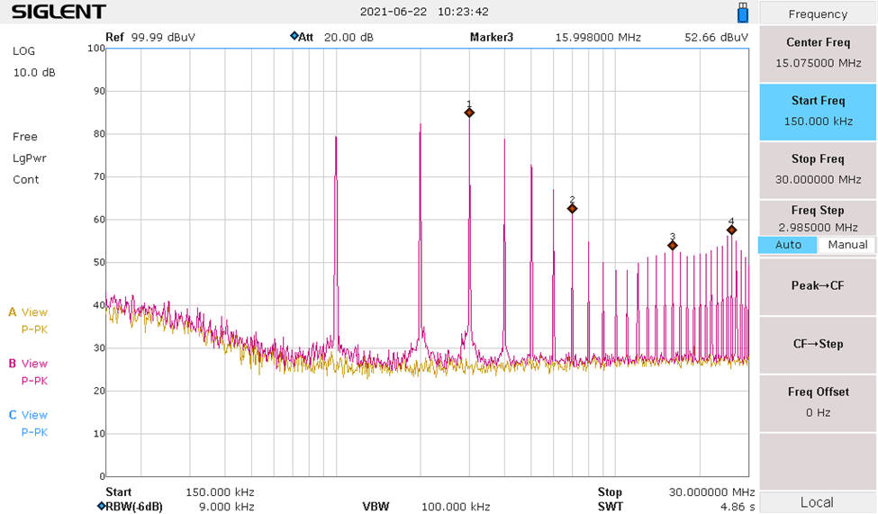
Figure 12. A typical data capture using the four available markers on various peaks across the spectrum. Here, we’re looking from 150 kHz to 30 MHz using the LISN to show the conducted emissions harmonics.

Figure 13. A typical data capture using the four available markers on various peaks across the spectrum. Here, we’re looking from 30 to 150 MHz and using the LISN Mate to show the differential mode harmonics.
Test Procedure – Field Mapping
The Y.I.C. Technologies EMScanner comes with custom software to make automated measurements of harmonic energy versus frequency (spectral display) and a heat map of the measured H-field emissions and current flow around the board. Once the board under test is positioned on the scanner array and the area of the board is defined and the associated software is activated, results of these smaller boards are available within a few seconds.
I chose to display both the spectral and spatial (heat map) data across two different frequency bands (150 kHz to 30 MHz and 10 to 300 MHz).
Results
In each case, the blue trace indicates the solid return plane (board 1-1) and lower in the plot is better (lower EMI).
LISN Conducted Emission on Vin (test setup in Figure 6)
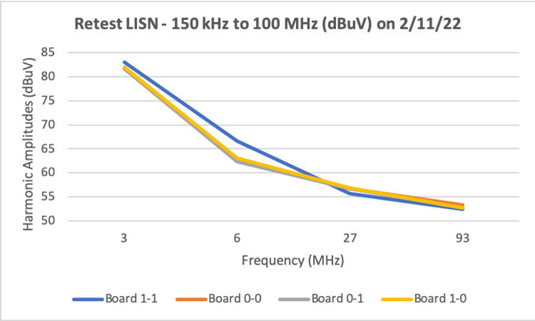
Figure 14. This result surprised me; it doesn’t track well with the other methods of measurement. We can plainly see that the solid board (1-1) is a few dB worse from 3 to about 20 MHz, after which, there appears to be little difference in the four boards. This test was repeated multiple times to ensure consistent measurement results.
Current Probe on Vin (test setup in Figure 7)
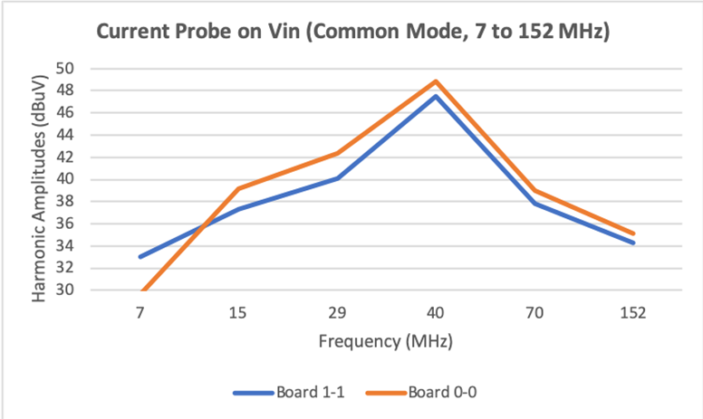 Figure 15. With the RF current probe measuring the common mode currents on the Vin cable, and comparing the solid plane (1-1) to the completely cutout plane (0-0), we see that at most frequencies above 10 MHz, the solid plane had an advantage by 1 to 2 dB less emissions (blue line). Frequencies below 10 MHz were much more variable with inconsistent results.
Placing an RF current probe on a cable and measuring the minute RF currents relate to radiated emissions, using a well-understood E-field equation as described in Workbench Troubleshooting EMC Emissions (Volume 2) [4], implies that radiated emissions might be slightly lower with the solid return plane.
LISN Mate – Differential Mode (test setup in Figure 8)
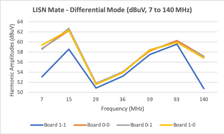
Figure 16. When the differences in differential mode currents were measured, there was a clear advantage in using the solid return plane. Differences varied between 0.5 and 6 dB, depending on frequency.
The advantage in splitting out the differential and common mode noise currents is that you can evaluate the input filter sections more intelligently. This is a significant advantage specifically for designing the input EMI filter. In Figure 16, we clearly see the differential mode noise currents are greatly affected by the solid return plane, while in Figure 17, the common mode noise currents are affected less so by a solid plane.
LISN Mate – Common Mode (test setup in Figure 8)
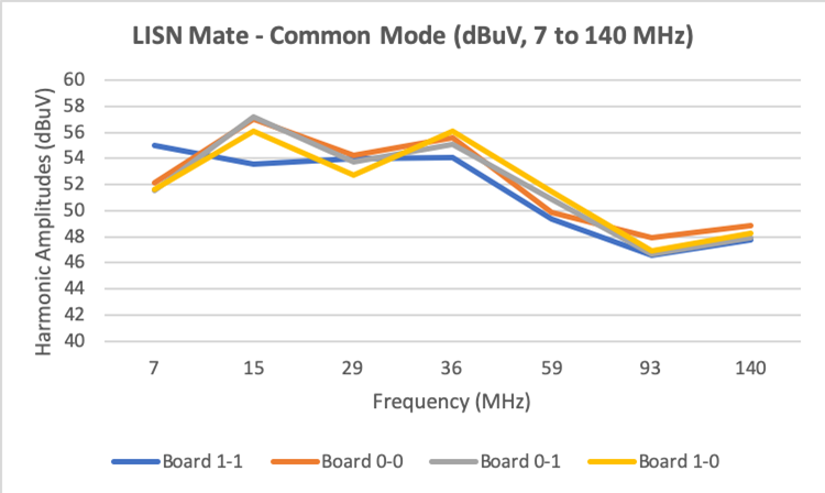
Figure 17. When the differences in common mode currents were measured, there was not as clear an advantage in using the solid return plane at all frequencies. However, there were differences noted at 7 MHz and from 36 to about 80 MHz. Differences between the solid plane and others varied between 0.25 and 2.5 dB, depending on frequency.
Y.I.C. Technologies Field Scanner – Radiated Fields (test setup in Figure 9)
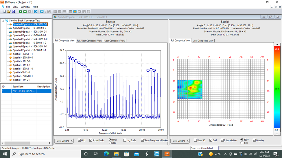
Figure 18. Looking from 150 kHz to 30 MHz, the fully-voided board (0-0) has several hot spots under the inductor and switch node, and the emissions from the bottom are peaking at 30 dBµV.
In Figure 18, this screen capture from 150 kHz to 30 MHz shows the spectral response on the left, and the spatial “heat map” of the high frequency currents flowing around the board on the right. As we see, the fully-voided board (0-0) displays high 1 MHz switching frequencies in the spectral display and several “hot spots” indicating high frequency electromagnetic fields and associated currents flowing around the bottom of the board.
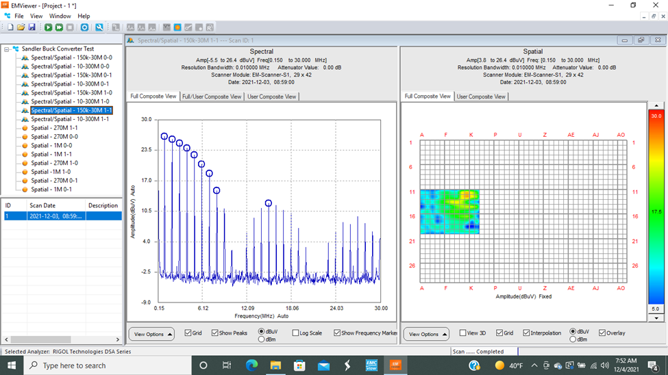 Figure 19. Looking from 150 kHz to 30 MHz, the solid board (1-1) looks relatively quiet; the emissions from the bottom are reduced by about 5 to 10 dB.
Figure 19 is the same capture using the solid return plane (board 1-1). The spectral response is 7 to 10 dB lower and the spatial response shows lower fields and associated high frequency currents flowing on the board.
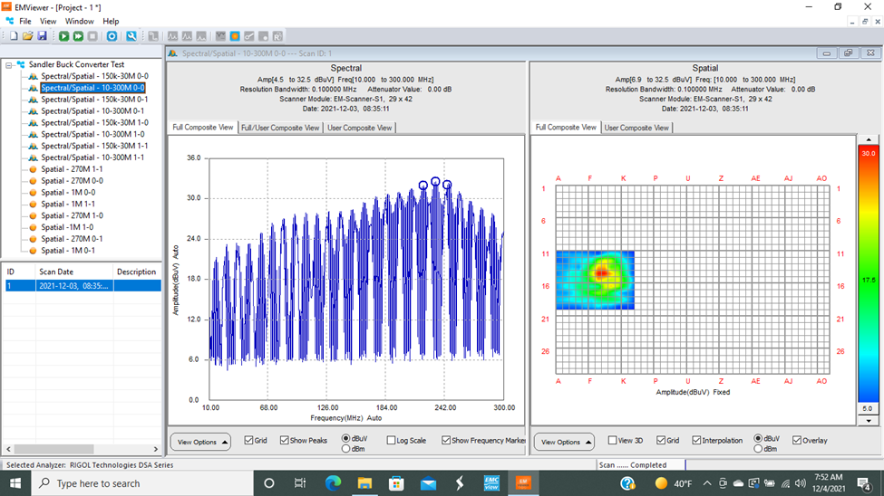
Figure 20. Looking from 10 to 300 MHz, the fully-voided board (0-0) has a strong hot spot under the inductor and switch nodes and the emissions from the bottom are significantly higher, peaking about 33 dBµV.
In Figure 20, we’re now looking from 10 to 300 MHz, as I wanted to capture a known resonance due to a 270 MHz ringing on the switched waveform. The fully-voided board (0-0) shows very high spectral harmonics and a defined hot spot under the switch node and inductor.
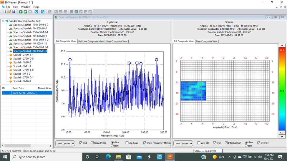
Figure 21. Looking from 10 to 300 MHz, the solid board (1-1) looks benign and the emissions from the bottom are reduced to 13 dBµV, or 20 dB lower.
Figure 21 is the capture for the solid return plane (board 1-1) from 10 to 300 MHz and clearly shows a 20 dB decrease in harmonic energy from 100 to 300 MHz in the spectral display and few high frequency currents in the spatial display.
Conclusions
At frequencies above 10 MHz, it seems clear that conducted emissions with a solid return plane is equal to, or better, than a return plane with cutouts (at most frequencies). At frequencies below 10 MHz, the difference was not so clear.
I’m not sure why the standard conducted emissions test using the LISN did not appear to track well with the other test results. This testing was repeated several times to ensure repeatability. Although, I have to note that the other test results below 10 MHz did appear variable, or seemed to indicate the solid return plane was also relatively inferior in some cases.
As expected, the electromagnetic field scanner clearly showed less harmonic energy and lower high frequency currents at the bottom of the board with the solid return plane.
It’s useful to realize this data is only valid for this buck converter and this board design. Other DC-DC converter topologies, and those operating off-line with much higher primary voltages, may differ greatly in results and conclusions.
Based on the above results, I’m inclined to recommend that a solid return plane be used for all DC-DC power conversion. In cases below 10 MHz where the solid plane seemed inferior, it was usually only by 2-3 dB.
Acknowledgment
I’d like to thank Steven Sandler, of Picotest, for designing and producing the four sample PC boards for this evaluation and for his technical assistance. According to Steve, this was intended to be an open source project, inviting others to participate. To that end, the discussion is on the Picotest forum and on this page you can download for FREE the schematics, BOM, GERBER files, ODB++ simulation files. Those wishing to repeat these tests, Picotest has a limited quantity of blank boards available for sale. Contact Steve directly for information.
A related article addresses selection of the switching inductor. The inductor used in this experiment had a relatively high capacitance and likely radiates pretty well.
My colleague, Andy Eadie, of EMC FastPass, has also evaluated these boards and compiled the results in a video [7].
References
- André and Wyatt, EMI Troubleshooting Cookbook for Product Designers, SciTech Publishing, 2014.
- Sandler, Power Integrity – Measuring, Optimizing and Troubleshooting Power-Related Parameters in Electronics Systems, McGraw-Hill, 2014,
- Wyatt, Create Your Own EMC Troubleshooting Kit (Volume 1), 2nd Edition, WTS Publishing, 2022.
- Wyatt, Workbench Troubleshooting EMC Emissions (Volume 2).
- Wyatt, Design PCBs for [Low] EMI – Part 1 (in four parts, other parts linked), EDN.
- Wyatt, Review: Tekbox LISN Mate is Valuable for Evaluating Filter Circuits, EDN.
- Eadie, DC-DC Converter Layout – Solid Ground Plane or Cutout Below Switch Node? (video).