
What does it take to design predictable PCB or packaging interconnects operating at tens of Gbps? Properly identified dielectric and conductor roughness models, known manufacturer geometry adjustments, properly validated simulation tools – those are necessary conditions. An often forgotten necessary condition is the localization property: to be predictable, all elements of an interconnect link must be localized up to a target frequency! This article introduces and illustrates the localization concept with the power flow density computed using the Trefftz finite element solver in Simbeor THz software.
Ideally, all interconnects should look like uniform transmission lines (or waveguiding structures) with the specified characteristic impedance. In reality, an interconnect link is typically composed of transmission lines of different types (micro-strip, strip, coplanar, coaxial, etc.) and transitions between them, such as vias, connectors, breakouts and so on. Transmission lines may be coupled to each other, causing crosstalk. The transitions may reflect and radiate energy due to discontinuities in signal and reference conductors. The crosstalk, reflections and radiation cause unwanted and sometime unpredictable signal degradation.
If analysis of traces or viahole transitions is possible in isolation from the rest of the board up to a target frequency, the structure is called localized (see more at app notes #2009_05 and #2013_05 at http://www.simberian.com/AppNotes.php). This means all the important contributions to the signal and return currents, and their associated power flows are confined to the region of the geometry included in the analysis. If a fraction of the return currents or signal power flows out of the geometry analyzed, the problem is not localized, and the simulated results are not accurate.
Structures with behavior dependent on other structures and on-board geometry are called not localized, and they should generally not be used in multi-gigabit interconnects. Examples of non-localized structures are coupled traces, strip lines with reference planes not connected to each other, traces crossing gaps in reference planes, and vias with far, no or an insufficient number of stitching vias (vias connecting reference planes of the connected traces). Analysis of non-localized structures is usually possible only at the post-layout stage with substantial model simplifications that degrade accuracy at higher frequencies.
To design predictable interconnects, only localized structures must be used– this is one of the most important elements for design success. The localization is always bandwidth limited for strip lines (two reference conductors) and for vias (two or more reference conductors).
Localization is not only important for accurate simulation, it is also a good engineering practice. Designing interconnects with localized properties means they do not interact with distant features of the boards. This results in more predictable and robust interconnects, especially for higher bandwidth applications.
How do you estimate the localization property of a transition?
One way is to run an electromagnetic analysis of the structure with different boundary conditions, or simply change simulation area size without changing phase reference planes and evaluate the differences in the computed S-parameters. If the difference is small, the structure may be considered localized and suitable for final design (see more at app note #2013_05). Or, you can compute and plot power flow density and literally see the localization of the signal in space as illustrated here.
First, let’s get familiar with the power flow density concept using a simple example and analogy with the circuit theory for a strip line structure:

Voltage in circuit theory corresponds to the modal electric field intensity E. Current in circuit theory corresponds to the modal magnetic field intensity H. The cross-product of the electric field and magnetic field intensities is the vector of power flow density (or Poynting vector), measured in Watt/m^2. It is the energy through a unit area in space transferred in 1 sec. When we look at the power flow density vectors, we basically see where the energy of the signal is located in space around a trace or via-hole. Total power through a cross section of a strip line corresponds to the power flow in the corresponding transmission line model, equal to the product of the voltage and current.
To understand the localization concept, it is very important to know that the signal energy is actually distributed in space around each element of the interconnect structure. For instance, the power flow density of the dominant quasi-TEM mode in strip line is shown below at 4 frequencies:

The strip is 1.2 mil thick, 7 mil wide trace, in homogeneous dielectric with Dk=3.76, Loss tangent = 0.006 @ 1 GHz, planes 0.77 mil thick and 17.2 mil apart, 1 V excitation and 50 Ohm terminators.
The power flow density is depicted by vectors with the direction along the t-line (into the picture) outside of the conductors. The magnitude of the vectors is expressed with color scale in dB from zero (red color) to -60 dB (blue color). Note that the magnitude of the power flow is color coded in a dB scale. A -3 dB drop is a factor of 0.5 and a -20 dB drop is a factor of 0.01 in power flow. The red color shows that most of the power is flowing down the transmission line in close proximity to the signal line, but its precise distribution depends on frequency.
We can observe that the maximal power density is uniform around the strip at lower frequencies and concentrates around the strip edges at higher frequencies. As we can also see, the power of the signal drops around the strip rather quickly to -50 dB (by 0.00001 times). We can say that the structure is well localized if there is nothing in the area with significant power flow (no coupling to the other strips for instance).
However, the localization is conditional on homogeneity of dielectric and uniformity of the strips. If such conditions are not satisfied (and they are usually not satisfied for PCB interconnects – dielectrics are not homogeneous and there are large variations in manufacturing), the energy of the quasi-TEM mode can be transformed into the dominant TEM wave of the parallel plate waveguide formed by the top and bottom plane. This is a form of mode conversion. Some of the signal propagating in the TEM mode of the transmission line can be converted, by asymmetries and non-uniformities, into the TEM mode of the parallel plate waveguide mode. To avoid this mode conversion, stitching vias connecting the planes should be used along the traces at higher frequencies.
The distance between the stitching vias should be less than half of wavelength in dielectric at the highest frequency of interest – that may be a lot of additional vias. The strip line localization can be easily violated if the equipotentiality of the reference planes is not ensured with the stitching vias. The result is the signal energy leak along the trace (can be observed on TDR as flat or decreasing impedance). Due to reciprocity, this works both ways – the energy of the power distribution network, when the two planes in the stripline are different voltages,can be coupled to the trace, if it is not localized with the stitching vias.
Now let’s take a look at the power flow density in via-holes. One of the links on EvR-1 board, designed by Marko Marin and described in our award-winning DesignCon2018 paper, M. Marin, Y. Shlepnev "40 GHz PCB Interconnect Validation: Expectations vs. Reality,” had two single-ended vias specifically to test the localization importance. One of the vias has two stitching vias at about 30 mil distance from the signal via and another has no stitching vias in the vicinity as shown below:

The through via with two adjacent return vias was localized, while the signal via with no adjacent return vias was not localized.
We used the "sink or swim" formula for predictable interconnect design that is based on these components: interconnect geometry adjustments + identified material models + validated software -> predictable interconnects. With all three components in place, we were able to reliably predict the behavior of most of the interconnect structures on the EvR-1 board without additional tuning or calibration for 28-30 Gbps NRZ signal.
However, the analysis to measurement correlation was acceptable only up to about 5 GHz for the structure with the non-localized via shown above. Non-localization makes it predictable for signals with only about 3-5 Gbps data rate. The TDR plot shown below reveals the large discrepancies in the measurements, and the model at the location of the single via without the stitching vias. We can see some oscillations at the via location. It means that the via is coupled to a resonating cavity formed by parallel planes and multiple distant vias around the traces.

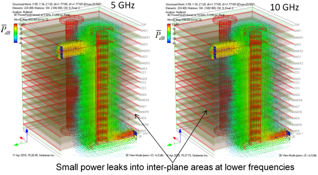
To see how the coupling happens, let’s use the power flow density visualization. A 1 V signal source is connected to the microstrip line port at the bottom of the board. Both microstrip and strip line ports are terminated with 50 Ohm. As we can see, the power from the microstrip line at the bottom does not go all the way to the strip line in the layer INNER1 – some energy is radiated into the inter-plane areas as shown below for 5 GHz (peak values of the power flow density):

This model uses absorbing boundary conditions on the outside boundaries of the simulation domain; it absorbs the energy of the parallel plane waves going from the via. For instance, here is the close up of what is going on between the reference planes GND7 and GND8 – the power flows along the via in the anti-pad area and flows mostly outward between the parallel planes and is absorbed at the outer boundary:

In reality, the energy injected into the inter-plane area does not completely disappear. It may be reflected from the fences formed by vias and returned back to the signal via in form of the oscillations observed on TDR above (coupled to cavities formed by distant stitching vias). Behavior of such vias can be predicted only in the post-layout analysis with either huge computational cost (large simulation area) or with simplified models of the whole board with substantial model accuracy degradation. The easier alternative and more robust and predictable design, is to localize it!
The second via in this link was designed to see how effective would be 2 stitching vias placed at about 30 mil from the signal via. The TDR correlation for this via is acceptable, let’s see how the power propagates along that structure at different frequencies:

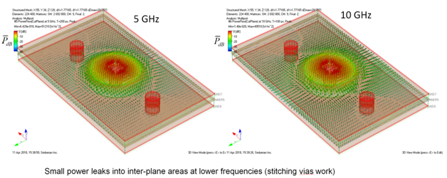

What a difference just two properly designed stitching vias make! The localization bandwidth of the single via is extended to 15-20 GHz. The localization degrades progressively starting from about 20 GHz in this case – it means that this via becomes coupled to the parallel plane structures with all the unpredictability consequences as we observed for the single via. What if we want to extend the frequency range further up to 50-60 GHz? That is a very difficult task for the single-ended through vias in general. Just take a closer look at an example of the single via launch localized up to about 60 GHz with 17 stitching vias as shown below:
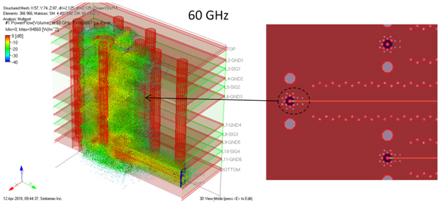
This via transition was designed by Scott McMorrow for one of our material model identification projects reported in D. Dunham, J. Lee, S. McMorrow, Y. Shlepnev, 2.4mm Design / Optimization with 50 GHz Material Characterization, DesignCon2011. It is also featured in demo-video #2018_01 (demo-videos #2016_01 and #2018_01 use power flow density to illustrate the effect of the stitching via number and positioning).
Summary and Conclusion
The bottom line is that the possibility to simulate a link in isolation from the rest of the board, or localization, is probably the most important, necessary condition to design predictable interconnects. Only structures with behavior predictable up to a target frequency should be used to design links for tens of Gbps data rate. The closeness of the stitching vias should be measured relative to the wavelength. The stitching vias can be considered close as long as the distance does not exceed a quarter of the wavelength at the target frequency. The number of stitching vias also matters. Without localization, the interconnects cannot be accurately simulated in most of the practical cases. If an interconnect’s behavior cannot be predicted, the outcome is uncertain: it may work or may fail!