
At the last “normal” DesignCon in 2020, our Simberian booth was next to a booth with a very loud demonstration transferring 112 Gbps over a distance of about 1 meter through cables. I do not know how many terabytes of data they transferred during the show, but the demonstration equipment was very noisy due to the industrial cooling equipment. One could literally feel the heat coming out of it and, apparently, the devices were just transferring the data and doing nothing else. So, I started wondering how much energy is required to transmit the data and why so much power is dissipated into heat?
Energy per Bit
First, let’s begin with the simple evaluation of energy absorbed (or dissipated) by copper interconnects. The power delivered to a 100 Ohm differential transmission line with 1V signal amplitude is 10 mW. It doubles to 20 mW if the transmitter source termination resistor is taken into account. Let’s assume that the link is ideally designed as in Figure 1 - no reflections and coupling (such links can be designed indeed). The remaining signal degradation factor is the absorption or dissipation – losses in conductors and dielectrics and dispersion related to it.
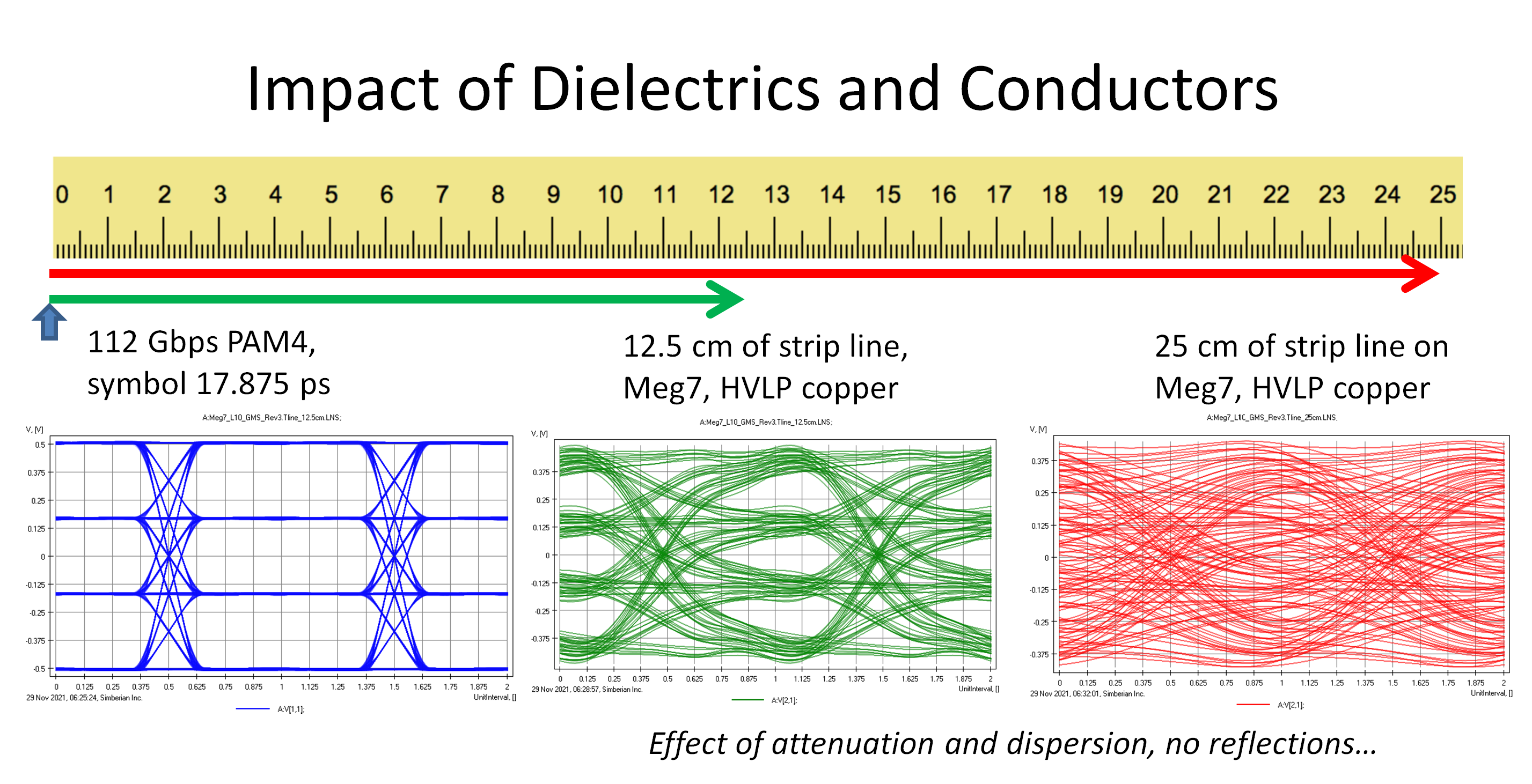
Figure 1: 112 Gbps PAM4 signal degradation in a typical PCB interconnect due to absorption in dielectrics and conductors.
So, if the link insertion loss due to absorption at the Nyquist frequency (half of the bit rate for the NRZ signal) is -20dB, then we have only 0.1 mW at the receiver end (0.1 V, 100 Ohm). Note that receivers on some expensive components allow -30 dB (0.032V, 10 uW) and even -40 dB (0.01V, 1uW) loss at the Nyquist frequency. Actually, it does not matter for our evaluation, because the signal at the receiver end is also converted into the heat at the termination resistor. It basically means that all signal energy is converted to the heat!
For a 50 Gbps NRZ signal with 20 ps unit interval, the energy converted into heat in a differential link with termination resistors is about 0.4 pJ/bit (20 mW x 20 psec - product of power and bit time). This is practically an immutable bottom level – we cannot reduce the energy per bit in the copper interconnects under the assumptions provided above (1 V, 100 Ohm). 20 mW of power or 0.4 pJ/bit for 50 Gbps NRZ signal – is it small or not? It would take almost 929 hours to boil one cup of water (heat 200g of water from 20 to 100 deg. C). Admittedly, it does not look like much heat. However, this is just one link, and internet routers or switches may have more than one thousand such links – that is enough to have a cup of tea in about 1 hour. It is still not impressive.
But, this is not the end of the story. When equalization is included, the actual cost of a bit transfer on a PCB for 50 Gbps is at least an order of magnitude larger – it is about 5 pJ/bit (or 250 mW) for 50 Gbps NRZ [Stauffer,2014]. With a thousand of links this is enough to prepare a cup of tea in 5 min! And about 90% of this energy is dissipated by the IOs on chip.
Does this explain the industrial cooling equipment for 112 Gbps links? I have not seen the power consumption data for 112 Gbps or the upcoming 224 Gbps links (ping me if you do have it). But, following the recent trends (doubling data rate increases required power by 30%) it should be about 6.5 pJ/bit (325 mW) for 112 Gbps and 8.45 pJ/bit (422 mW) for 224 Gbps.
The number of IOs does not increase at the same time – that may be the clue. Also, the prototype equipment may be much less efficient. On the bright or cool side, some recent developments in this area promise to reduce the numbers to about 2 pJ/bit or 100 mW [Razavi, 2021].
Why do we need so much power? To mitigate the signal degradation in interconnects between the driver and receiver. Transmitters and receivers are not 2-transistor devices in serial interconnects; they contain hundreds (may be even thousands) of transistors and most of the energy is spent to generate and restore the signal. Can we reduce the power by design of interconnects? The answer is absolutely yes, by reducing the signal degradation in interconnects!
Energy loss in dielectrics
In general, more power and more expensive components are required for interconnects with larger loses or overall signal distortion, and lower power is needed for interconnects with smaller losses and distortions.
During a tutorial at DesignCon 2020 [1] we discussed the major signal degradation factors and how to reduce them or design “transparent” or “clean” interconnects. The degradation factors can be broken into three categories: (1) absorption or dissipation by conductors and dielectrics and dispersion related to that, (2) reflections, and (3) coupling.
We called the first category “thermal losses,” because the signal energy is literally heating the interconnect materials. Though, maybe “absorption” or “dissipation losses” are better terms, and this article is about this topic.
When performing interconnect modeling, the following questions should be answered: What effects are important at a particular data rate? Are they accounted for by signal integrity software? If all effects are included, will the model correlate with measurements?

Figure 2 : Properties of dielectrics and conductors.
Electrical properties of dielectric and conductive materials are outlined in Figure 2. Let’s start with the energy absorbed (or dissipated) by dielectrics and the dispersion related to it. Why does the dielectric matter? Because the signal energy propagates along the PCB and packaging interconnects mostly in the dielectrics around the signal conductors. As Ralph Morrison pointed out “Energy travels in the spaces, not in the traces.” The signal energy location can be illustrated with the peak power density flow (PDF), a vector product of electric and magnetic fields. For a typical PCB stripline interconnect, shown in Figure 3, the color scale is used to plot peak power flow density (PFD) in W/m^2 (shown in dB), computed with Simbeor THz).
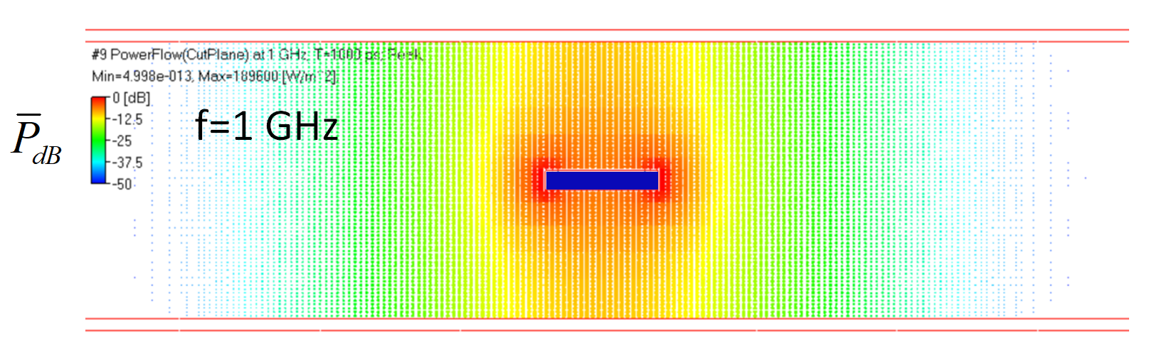
Figure 3 Caption: Power flow density in a typical PCB stripline interconnect (strip 1.2 mil thick, 7 mil wide, DK=3.76, LT = 0.006 @ 1 GHz, planes 0.77 mil thick, 17.2 mil apart)
We can see that the signal energy concentrates near the strip edges and between the strip and planes in the dielectric. The PDF is directed along the conductors into the picture. There is actually no power moving in the direction of the signal within the conductors. All dielectrics absorb or dissipate the energy – it is important to understand it (this was subject of another tutorial [2] from DesignCon 2016).
In general, dielectric properties can be described with the permittivity that is a complex function of frequency (always for real materials!). We call the real part of the permittivity the dielectric constant (Dk). The ratio of the negative imaginary part of permittivity to the real part is called loss tangent (LT) or dissipation factor (DF). It describes the power loss to heat and dispersion. A universal dielectric model may look like the one in Figure 4:
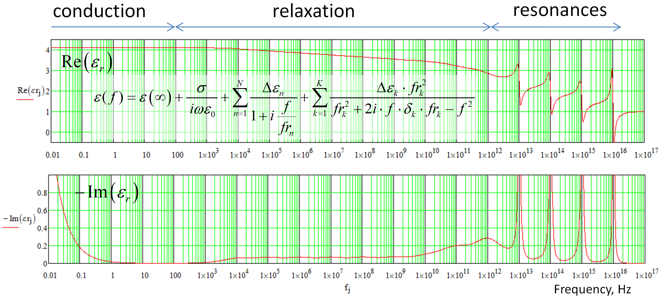
Figure 4: A universal dielectric model (real part is the top graph and negative imaginary part is the bottom)
The model in Figure 4 is actually of a real material up to 50 GHz (constructed from fitting measured data) and guessed above it. This is just to show the different mechanisms contributing to the losses in dielectrics (imaginary part of permittivity) and dispersion.
The conduction losses for the dielectric materials in the PCB and packaging dielectrics are negligibly small. They are responsible for the increase of the imaginary part below 100 Hz (this is not a typo). There are very few free charges in the dielectrics, such as ionic carriers.
At frequencies up to 1 THz we are dealing with the relaxation of losses related to electronic polarization of atoms (RC type of circuit – no oscillations). That is modeled as either multipole Debye or wideband Debye models [2]. That also means that the Dk can only decrease with the frequency at these frequencies. We are dealing with composite solids here, mostly polymers. Lorentzian terms (oscillating RLC type of circuit) are added for illustrative purposes to show that the resonant properties of the solid PCB materials are important over 1 THz where Dk may go down because of the resonances.
A Causal Material Model
At “normal” frequencies up to 100 GHz, dielectric polarization losses can be accurately simulated with the pole-continuous or wideband Debye models. Attenuation per meter from the dielectric in some PCB materials in a typical stripline is computed and shown in Figure 5. The attenuation shows an approximately linear dB/length growth with frequency.
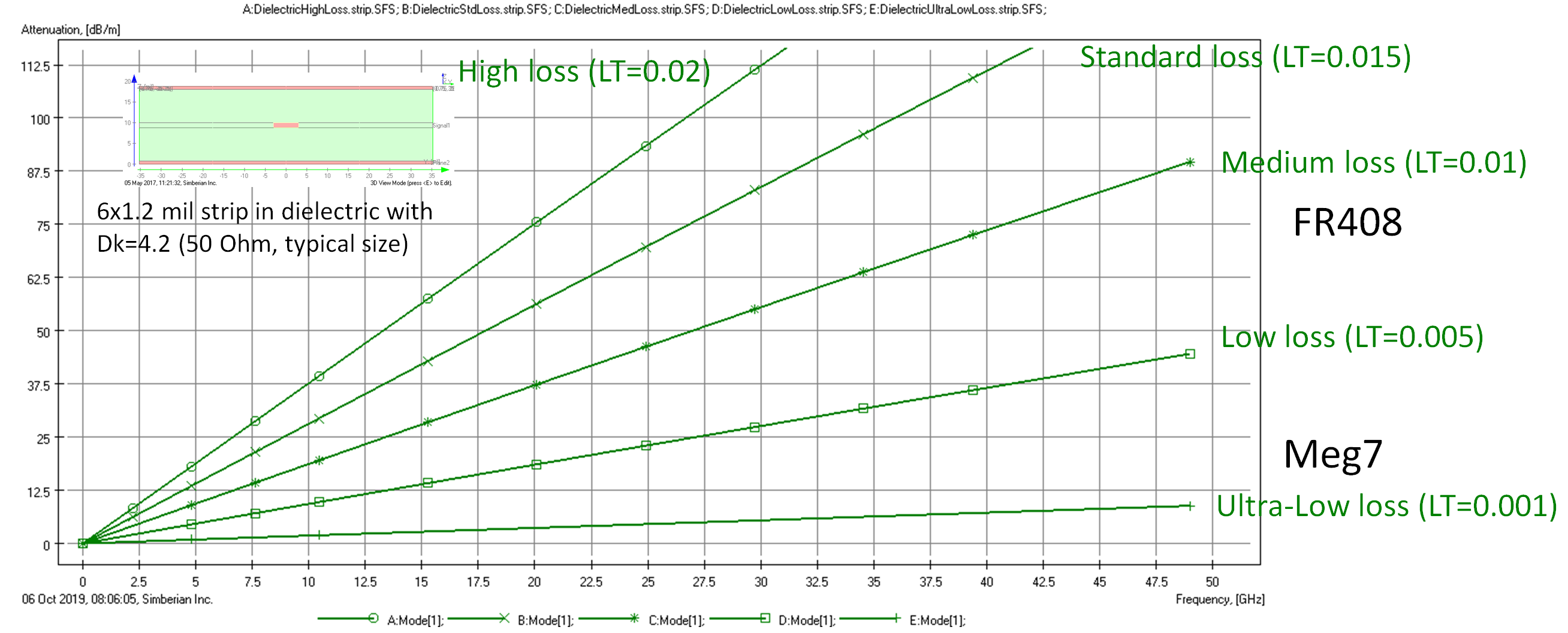
Figure 5: Attenuation per meter from different dielectric materials in a typical stripline.
As we can see the dielectric choice may have the most profound consequences on the link performance. For 112 Gbps PAM4 link, for example, the losses per meter at Nyquist frequency 28 GHz (quarter of bit rate or half of baud rate) may range from 5.1 dB/m for the ultra-low loss dielectric to over 100 dB/m (practically complete loss of signal) for the regular FR-4 type high loss dielectrics. Note that the ultra-low loss dielectric with LT=0.001 is still much more lossy than dielectrics used in cables. This is important to know when you make decision on switching from PCB to cables – there are many ways to reduce the losses on PCB interconnects.
A causal wideband Debye model is used here [2]. It can be defined with Dk and LT at one frequency point. 1 GHz in this case. The model analytically defines the dielectric constant and loss tangent dispersion from 0 up to 100 GHz. The model is causal and includes the dispersion (change in Dk with frequency) of the phase delay and characteristic impedance as illustrated in Figure 6.
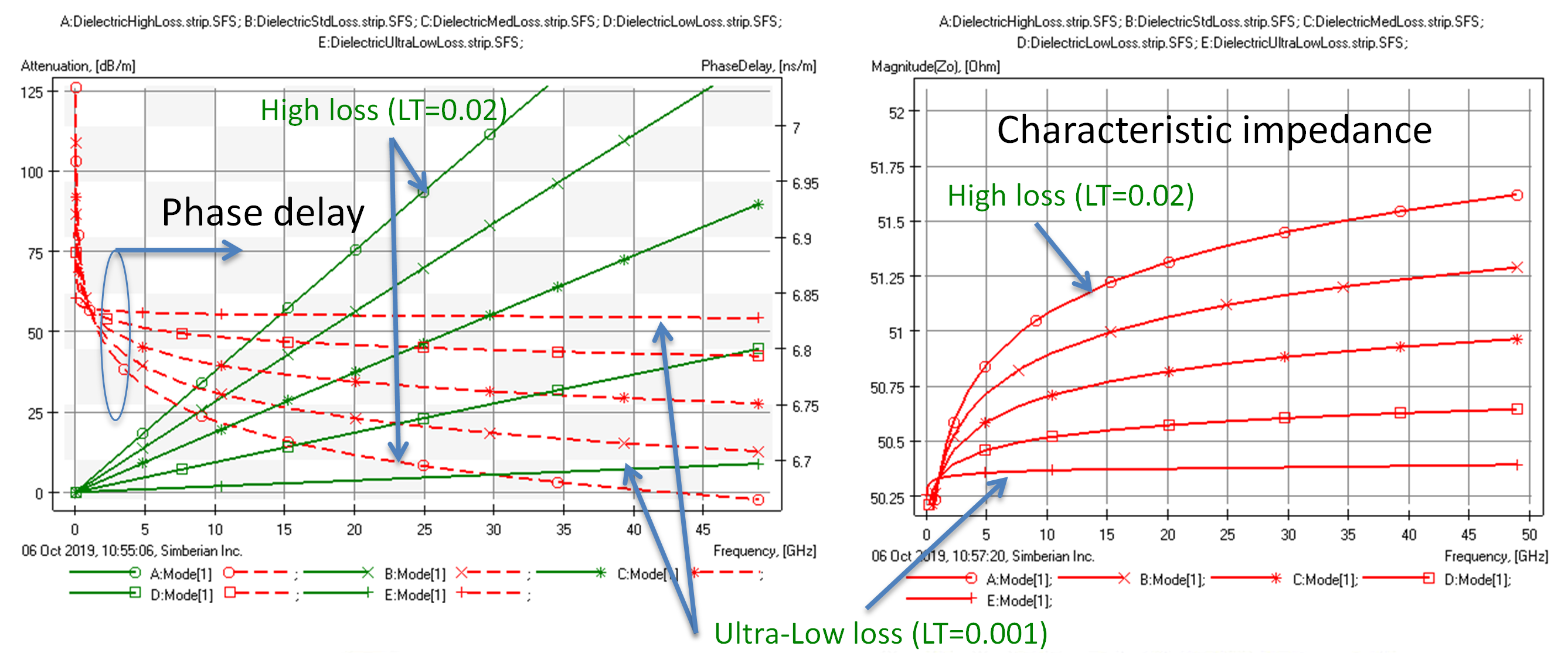
Figure 6 : Dispersion of phase delay (left graph, red lines) and characteristic impedance (right graph) for dielectrics with different losses (green lines on the left graph).
Phase delays are plotted on the left graph on the right axis in ns/m. Characteristic impedances are shown on the right plot in Ohm. This simple numerical experiment demonstrates that not only are the frequency-dependent losses included in the model, but it also captures the dispersion of phase delay and characteristic impedance. The model is not causal if it does not include such dispersion.
It also demonstrates that dielectrics with high losses (typical FR-4) have much higher dispersion compared to the ultra-low loss dielectrics that do not show much dispersion at the frequencies important for analysis of multi-gigabit interconnects. This is not only for the frequency-dependent losses, but also phase dispersion cause signal degradation. Signal harmonics are attenuated more at high frequencies and travel with different velocities as well.
Losses in Conductors
Conductor losses were extensively covered in the tutorial [2] and another “How Interconnects Work…” paper [3]. In general, the conductor absorption and dispersion effects can be summarized and illustrated as follows in Figure 7.
Figure 7: Conductor absorption and dispersion effects.
Though the currents in the conductors flow along the signal propagation direction (and back), the power flow vectors within the conductor always point almost exactly perpendicular to the conductor surface. Conductors literally absorb or “suck” the energy of the signal and convert it into the heat. This is because it is the tangential component of the H field that propagates into the conductor that accounts for the power loss.
Though conductors are indispensable part of PCB interconnects (no viable alternatives so far), there are additional unavoidable losses and dispersion related to them. As in the case of dielectrics, the absorption can be illustrated with the losses per meter as shown in Figure 8.

Figure 8: Attenuation from typical conductor roughness (red plots) in typical strip line compared with the attenuation due to dielectric losses (green curves).
Dielectric losses for the medium and ultra-low losses are plotted on the same graph as green curves for the comparison. Three red curves are computed for strip width 6 mil (about 0.15 mm) – with smooth copper (no roughness), with STD or reverse treated copper (middle curve) and with HVLP copper roughness. Parameters for the roughness models are taken from validation projects and were identified with the measurements.
We can see that even with smooth copper, the conductor losses may exceed the dielectric losses for the ultra-low loss dielectric (valid for a particular cross-section). It means that the minimum possible losses on a PCB are limited mostly by the copper and copper roughness! To have the losses on the PCB closer to cables over similar bandwidth, larger, smooth traces must be used (it reduces current density and overall losses). Due to the causality requirements, the conductor losses cause dispersion of the phase delay and characteristic impedance as illustrated in Figure 9.
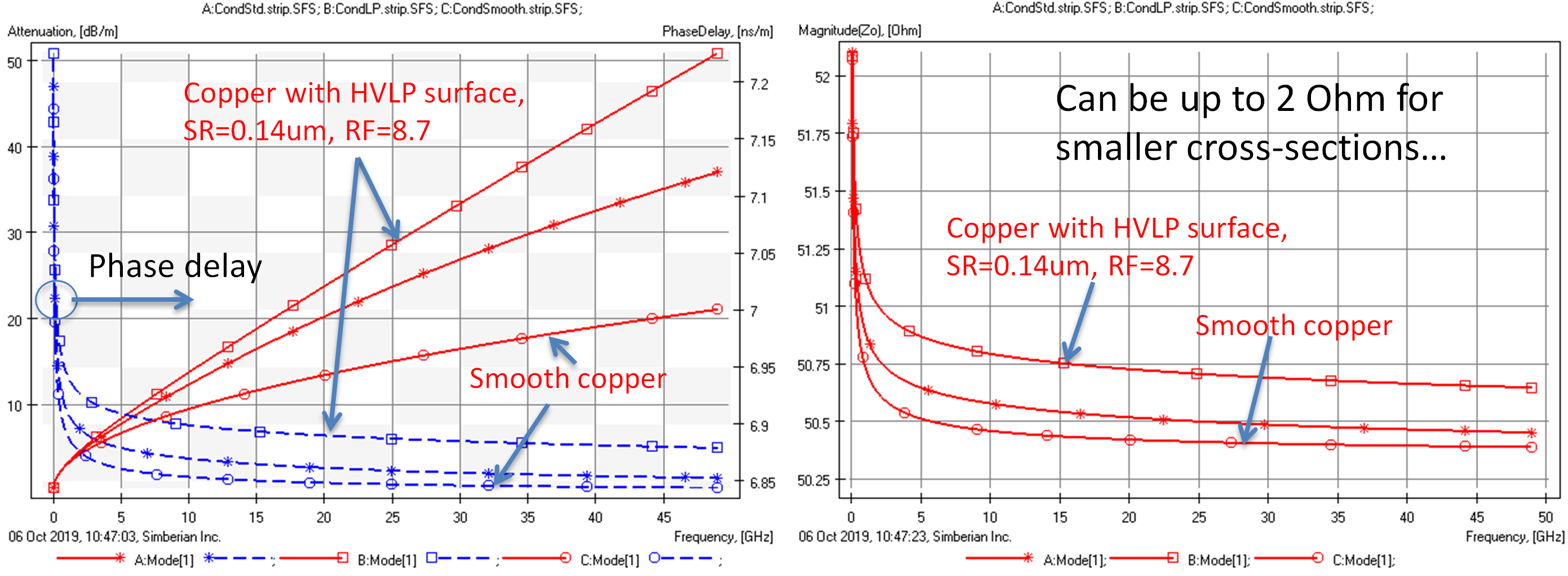
Figure 9: Dispersion of phase delay (blue curves on the left graph) and characteristic impedance (right graph) for different copper roughness (red curves on the left graph).
Again, if a model does not have the dependency of phase delay and impedance from the roughness model parameters, such a model is not causal and, thus, may be not be accurate enough. Always do numerical experiments to verify the dispersion associated with the frequency dependent loss, to see what is in the model. See more on the inductive effect of roughness in [3] and [4].
What about the predictability of the absorption or dissipation losses and dispersion? In other words, how do we build models that correlate with the measurements? It depends on availability of the frequency-continuous ultra-broadband models for dielectric and conductor roughness.
As was demonstrated in [2], dielectric data from laminate manufacturers can be used to construct such models with sufficient accuracy for preliminary analysis or lower data rates (can be defined with numerical experiment). Dielectric models for higher data rates and for better accuracy must be extracted from measurements. Parameters for conductor roughness models are usually not available and must be always extracted from measurements. Identification with GMS-parameters [5] or SPP Light [6] techniques with a separation of dielectric and conductor losses can be used to build dielectric and conductor roughness models. See more on the material model identification automation with Simbeor SDK at [7] and [8].
Conclusion: reducing power consumption
Here is how to reduce the signal degradation due to the absorption or dissipation losses:
- Use dielectrics with lower Dk and LT
- Use more metal to reduce current density – wider interconnect traces absorb less energy (subject to single mode propagation limit)
- Use conductors without roughness or “engineered” rough surfaces without additional losses
Energy of generated signals is always turned into heat in conductors, dielectrics or termination resistors, no matter what we do with the interconnect loses. However, interconnects with lower losses reduce the energy required for signal conditioning and restoration. This is valid under one important condition: very low reflections and no coupling. Those two signal degradation factors will be discussed in the next “How interconnects work…” articles.
Appendix:

REFERENCES:
- Y. Shlepnev, V. Heyfitch, Tutorial – Design Insights from Electromagnetic Analysis & Measurements of PCB & Packaging Interconnects Operating at 6- to 112-Gbps & Beyond, Tuesday, January 28, DesignCon 2020, Santa Clara Convention Center, Santa Clara, CA.
- C. Nwachukwu, Y. Shlepnev, S. McMorrow, A MATERIAL WORLD: Modeling dielectrics and conductors for interconnects operating at 10-50 Gbps, Tutorial at DesignCon2016, January 19, 2016, Santa Clara, CA.
- Y. Shlepnev, How Interconnects Work: Modeling Conductor Loss and Dispersion, 2016, Simberian App. Note # 2016_01.
- How Interconnects Work™: Rough conductor currents and internal inductance, Simberian video #2017_09.
- Y. Shlepnev, Broadband material model identification with GMS-parameters, 2015 IEEE 24st Conference on Electrical Performance of Electronic Packaging and Systems, 2015, San Jose, CA.
- Y. Shlepnev, Y. Choi, C. Cheng, Y. Damgaci, Drawbacks and Possible Improvements of Short Pulse Propagation Technique, 2016 IEEE 25st Conference on Electrical Performance of Electronic Packaging and Systems (EPEPS'2016), pp. 141-143, 2016, San Diego, CA.
- How to Identify Material Models for PCB & PKG Interconnects With Simbeor SDK, April 25, 2021, Simberian App Note #2021_03.
- Y. Shlepnev, Dielectric and Conductor Roughness Model Identification – Does Bandwidth Matter?, May 5, 2021, Simberian App Note #2021_04.