The risk of causing signal integrity, power integrity, and EMI problems with a split in the ground plane strongly outweighs the potential benefit; there is only one case when there might be a benefit for a split ground plane. It is explained here. Once connectivity is established, the only thing an interconnect is going to do is add noise. When an engineer designs interconnects, they must design them to reduce the noise they might generate. When making design choices, we are always asking the question, what is the noise problem we are trying to fix, and how do we engineer the interconnects to reduce this source of noise? If you are considering using a split ground plane, one must first answer the question, what is the problem a split ground plane is trying to fix? And what are the potential other problems that might be created, the law of unintended consequences?
Why Continuous Return Path Planes
The first step in engineering interconnects to reduce noise is to provide a continuous, low impedance return path to control the impedance, which controls reflection noise, and reduces the crosstalk between signals that share the same return conductor.
A wide, continuous ground plane adjacent to a signal trace will be the lowest crosstalk configuration. Anything other than a wide plane means more crosstalk between signal paths sharing this return conductor. This means never add a split or gap in the return path. That would run the risk of a signal trace inadvertently crossing this discontinuity.
If a signal crosses over a split ground plane, there are two effects that compound each other. Crossing a split creates a higher impedance path for return currents that must cross the split and forces return currents from multiple signals to overlap through the same higher impedance common path.
This creates the trifecta of problems: reflections from the return path discontinuity, ground bounce from the higher inductance return path, and EMI from the difference in potential between the two regions of the planes in which the return currents flow.
Therefore it is never a good idea to add a split in the ground return plane; you take a big risk of signals routed crossing this split.
However, there is one potential problem a split ground plane solves, provided the split or gap in the return plane is always parallel to the signal path, and return currents do not cross this gap. It is the minor issue of crosstalk from resistive coupling.
Where Return Currents Flow
The path return currents take in a ground plane depends on the routing of the signal paths. The signal and return paths cannot be considered separately; they are linked together. The path the currents take in a signal and return conductor are dictated by the path of lowest loop impedance. If there were a path the signal-return current took that was lower impedance, there would be a lower voltage drop along that path and currents would flow from the higher voltage paths to the lower voltage paths until all conductors, normal to the direction of propagation, were at an equipotential. This means that of the multiple paths signal-return currents could take, the currents will flow in the path to minimize the loop impedance of all possible paths.
Usually, the signal trace is narrow and confines the signal current to a very specific path. The return current can flow in the adjacent ground plane anywhere, unconstrained except for the plane edges. It will take the path so that the loop impedance of the signal-return path is minimized. To first order, the impedance of the signal return path is frequency dependent and related to:
In this equation, Z is the loop impedance of the current loop path, R is the series resistance of the loop, and L is the loop inductance of the path.
Imagine the signal-return path currents as composed of continuous current filaments taking any path they can down the interconnect. The filaments that have the most current are those with the lowest loop impedance. The more current flowing down one of these filaments, the higher the voltage drop across this series impedance. This pushes more current into adjacent higher impedance filaments until the cross section of current distribution, balanced by the impedance of each filament and the amount of current in each filament, create an equipotential across the direction of propagation.
There will always be a frequency, above which the ωL term dominates, and the current paths are driven by the path of lowest loop inductance. This is the region we refer to as the skin depth region. The current redistribution for lowest loop inductance is what drives the skin depth effect.
The lowest impedance path is when currents within the same conductor are farthest apart, to reduce the partial self-inductances, but are closest together between the signal and return paths, to increase the partial mutual inductances. This is illustrated in Figure 1, showing the current distributions in a simple microstrip at 1, 10, and 100 MHz; simulated with Ansys Q2D.
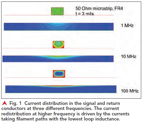
This means that in the high frequency regime, the return currents are always flowing directly underneath the signal currents. The path underneath the signal currents is always the lowest loop inductance path. Any current filaments away from this path will have a higher impedance, a higher voltage drop, and flow to the lower voltage filaments, directly under the signal.
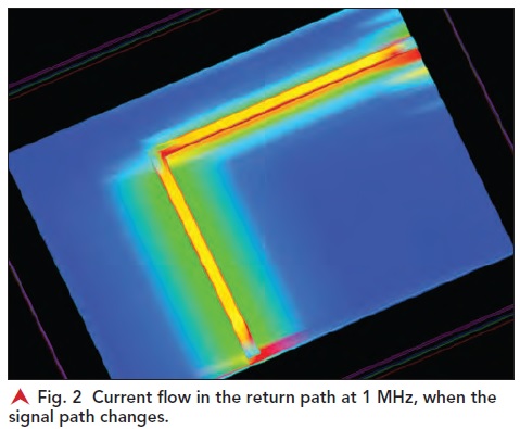
As the signal conductor meanders over the surface of the ground plane, the return currents will follow right along under the signal path. Figure 2 shows an example of the return current distribution in a plane when the signal conductor changes direction, simulated for 1 MHz frequency components.
Return Current at Low Frequency
At low frequency, when the loop impedance is dominated by the R term, the current distribution in the return plane is not driven by the loop impedance; it is driven by the loop resistance. In the signal path, the current will spread out uniformly as any filament path in the signal conductor will have roughly the same resistance.
But the current filaments in the return path with the lowest R will be those that are shortest. This means that return currents will take the shortest paths, independent of the signal paths. As frequency increases, the return current will redistribute to transition from the path of lowest R to the path of lowest L.
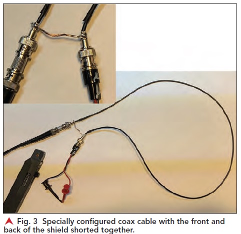
This was demonstrated in a simple experiment. A coax cable was shorted at the far end so that a DC current loop, driven by a function generator, would flow from the signal conductor and back through the return. At the front of the coax, the shield, which carries the return current, was shorted between the front of the coax and the back end of the coax as shown in Figure 3.
At DC, the return current will flow through the shunt between the front and back of the shield, which is a lower resistance path, instead of flowing all the way down the shield to the far end where the signal and return currents are shorted together.
To measure the current that flows through this path, a Hall effect current clamp was placed around this shunt path. This measures the current flowing through this specific path. The function generator was used to drive a constant 60 mA amplitude sine wave current through the coax cable and the frequency swept from 1 kHz to 10 MHz. The currents were measured with the Hall effect current probe and a Teledyne LeCroy Wave-Pro HD 12-bit, 8 GHz bandwidth scope.
At low frequency, all the return current flowed through the shunt path. But, as frequency increased, less current flowed through the shunt and more current flowed along the higher resistance but lower loop inductance path of the coax shield, with the return current in close proximity to the signal current.
Figure 4 shows the measured current amplitude in the signal-return loop at the far end, flat with frequency, and the measured current amplitude in the shunt, which drops off with a 1-pole response, above about 10 kHz.
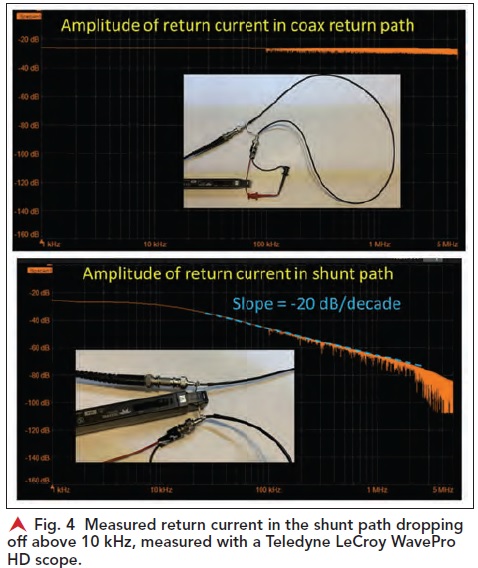
This illustrates that above about 10 kHz, all the return current will always flow in the path directly adjacent to the signal current to reduce the loop inductance of the signal-return path. But, equally important, the return currents below about 10 kHz will always flow in the path for lowest resistance.
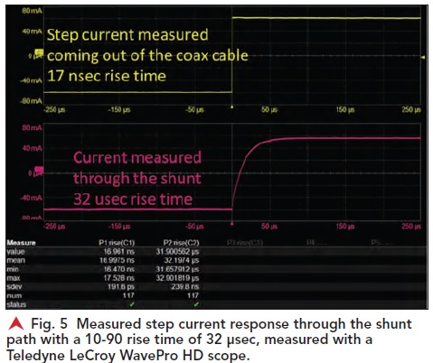
The transient step response of the current flowing through the shunt path will be a 1-pole response with a pole frequency about 10 kHz. This is an effective RC time constant of about 16 μsec. This would result in a 10-90 rise time of about 32 μsec. This is what is measured in the step response of the current through the shunt path, shown in
Figure 5.
Inductively Coupled Noise
In a plane, at frequencies below about 10 kHz, return currents will not flow under the signal path, but will spread out in the return plane. Above 10 kHz, the return currents are localized under the signal paths.
When we have two adjacent signal paths that are over a wide, continuous plane, they will show inductive crosstalk at high frequency. Even with minimal overlap of the return currents, there is still loop mutual inductance between the two signal-return paths. This inductive noise is driven by the changing current, the dI/dt, in the aggressor signal-return path, that will get smaller at lower frequency.
An aggressor signal with a transient, short rise time current edge will result in a noise signature on an adjacent victim line with a derivative of the aggressor current. The inductive noise would only appear synchronous with the switching current edge. Therefore, we call this sort of inductively generated noise “switching noise,” since it only occurs when signals switch transition levels. As the current change drops off with a lower slope, the inductive crosstalk drops off until it is below a measurement threshold.
This behavior was demonstrated in a simple board. In a two-layer board, we constructed six parallel, identical microstrip traces. One was the aggressor. Its far end was shorted to ground. A 2 kHz square wave of 120 mA peak to peak current was transmitted down the aggressor. The rise time was about 9 nsec, but the current was at a constant value for the rest of the period.
There were two victim traces symmetrically on either side of the aggressor. Between the aggressor and one of the victim lines, a gap in the return plane was cut. This isolated the return currents from the aggressor. They were unconstrained to one victim line, but eliminated from flowing under the other victim trace.
We expect to see switching noise on the adjacent victim trace that lasts only during the 9 nsec of the rise time. The rest of the period should show no switching noise. The measured switching noise on the two victim traces shows the impact from the gap in the return plane.
Figure 6 shows the measurement set up of the two configurations and the measured inductively coupled crosstalk on the two victim traces.
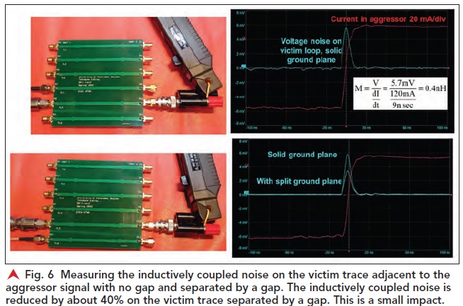
We see the signature of the switching noise as the derivative of the current edge. From the measured peak crosstalk (on the order of 5 mV in this example), rise time, and current peak, we can estimate the loop mutual inductance between the aggressor and the victim. With no gap, this is about 0.4 nH of loop mutual inductance. On the other side of the gap, it is reduced to about 0.25 nH. The gap redistributed the return currents and did reduce the loop mutual inductance to the victim trace on the other side of the gap, but it was by a small amount.