
Most modern circuit designs depend on accurate logic signals at the logic receiver. This assurance is based on the careful design of the signal path impedance, including printed circuit board (PCB) transmission lines, interconnects, vias, and cables.
If you have designed a controlled impedance transmission line based on a PCB stack-up, how do you know if the PCB fabrication house or another vendor built your stack-up to meet your controlled impedance specification? In fact, we have found, even after discussion with various laminate manufacturers, that the majority of dielectric constants specified in the vendor datasheet have uncertainty, with a lot of variability. This creates a call to action to measure these materials to get it right.
How a TDR Works
A time domain reflectometer (TDR) measures the reflections that result from a signal traveling through a transmission environment of some kind, such as a circuit board trace, a cable, a connector, etc. Since a TDR measures a voltage reflection profile with an oscilloscope, this profile can be converted to an impedance profile that allows measurement of a characteristic impedance and propagation delay of a transmission line. A TDR is a great tool that can be used to qualify vendor stack-ups, such as identifying the dielectric constant (Dk) variation of impedance.
Signal path length, signal propagation time, and dielectric constant (Dk) are all related. If we know any two of the three, we can use a TDR to solve for the third. Just remember the distance equals velocity multiplied by time. If we are using a defined structure where we know the physical length of the transmission line, then we can measure the propagation time and calculate the dielectric constant.
First, it is important to understand how a signal travels through a medium. To start, let’s re-iterate the definition of the speed of light in a vacuum, which is a constant shown by (1). This is also the speed a signal would travel in a vacuum.

With (1), we can calculate the phase velocity (Vp) of the signal transmission through a lossy medium, sometimes referred to as the velocity of propagation by:
From EQ(2), the signal travel time can be derived, which is defined as:
The TDR measures the reflection of the signal and so the signal has to make a round trip through the signal path. To determine the physical length of the transmission line, we divide by a factor of 2 for the one-way travel. This is shown in EQ(4).

Solving EQ(4) for Dk, results in EQ(5), which can be used to calculate effective Dk. The TDR is used to measure the signal round trip travel over a known distance. One of the signal paths (TP5-TP6) on the device under test (DUT), depicted by Figure 1, includes two “markers” exactly 3 inches apart, as marked on the silk screen.
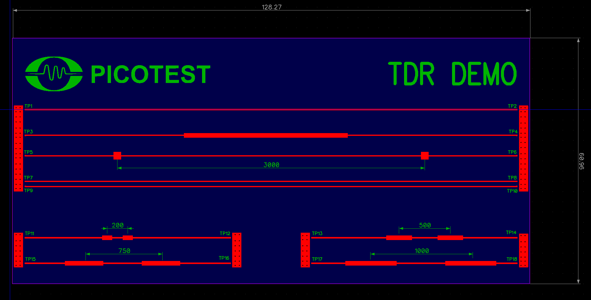
Fig. 1 - Depiction of Picotest TDR demo board included with the J2154A 12GHz differential TDR.
As a quick recap, a transmission line or waveguide consists of E and H fields defined by Maxwell’s equations. For a transmission line that consists of two or more conductors, the propagation mode is a transverse electromagnetic (TEM) wave. This is characterized by the fact that  and that the fields are similar in form to a plane wave in a homogeneous region [2]. This is important since the TEM wave propagation is the most common in PCB technology; however there are also other waves [3].
A microstrip consists of two conductors where the geometry is shown by Figure 2. A conductor of width (w) is printed on a laminate of defined thickness (h). With reference to Figure 2 and as defined in [2], if the dielectric constant (Ɛr) = 1, a two-conductor solution in a homogenous medium (air) would be presented. This would constitute a TEM transmission line with phase velocity
However, in a microstrip, the dielectric constant that the signal sees is not the bulk value of the laminate. Unlike in a stripline, the fact that a microstrip is not contained within a homogeneous dielectric region complicates things. The exact fields of a microstrip transmission line constitute a hybrid transverse magnetic-transverse electric (TM-TE) wave, which requires more advanced techniques for analysis [2]. To understand this, we need to think about how the electric (E) and magnetic (H) fields for a microstrip exist in a non-homogeneous dielectric. This is depicted by Figure 2.
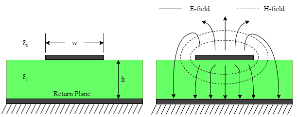
Fig. 2 - Geometry of a microstrip line and depiction of microstrip E and H field lines.
For more practical applications, as shown in [2], an approximation can be used for the dielectric constant. In this case, the signal sees an effective dielectric constant (effective permittivity Ɛeff) which is expressed by the approximation shown by EQ(6).

Simulation of the Laminate’s Dkeff
The Picotest TDR demo board shown in Figure 1 is a two layer PCB using Rogers RO4003C, which has typical Dk of 3.38+/-0.05 at 10GHz [4]. Since the demo board uses an 8 mil thickness laminate, the published bulk Dk is 3.803. Rogers Corporation also refers to the published bulk Dk as the Design Dk when using their MWI calculator. Per Rogers, there is no tolerance for Design Dk because it is dependent on thickness, copper type or surface roughness, frequency, and some PCB fabrication tolerances. The specified PCB stack-up for the TDR demo board is shown in Figure 3, and the specified trace width for the 3-inch trace labeled as TP5, shown in Figure 1, is 14.9 mils.
The TDR demo board, as shown in Figures 7 and 8, was cross-sectioned to determine the exact fabricated dimensions. The cross-sectioned results are shown below in Figure 4. With reference to Figure 3, the PCB is 2-layers, typically composed of a 0.203 mm thick RO4003C laminate with a 0.6 mm thick FR-4 backing, to get better stiffness and help prevent the PCB from curling. The total actual PCB finished thickness reported was 0.741 mm which is 62 um thinner than the specified total stack-up thickness. Unfortunately, from the reported cross-section, we do not know for sure the actual manufactured thickness of the RO4003C material laminate, FR-4 material laminate, or the variability of the laminate thickness. However, we do know the manufacturing tolerances for RO4003C as 8 mil +/- 1 mil (0.20 mm +/- 0.03 mm) [5]. These published manufacturing tolerances allow for a 12% variation in the laminate material thickness.
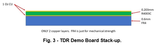
Fig. 4 - TDR Demo Board Cross Section Information.
As shown by Figure 5, the effective Dk for our PCB is simulated using the 2D solver that is within Controlled Impedance Line Designer (CILD) [6] as part of Keysight PathWave ADS. The result from ADS shows an effective dielectric constant of Dkeff = 2.869.
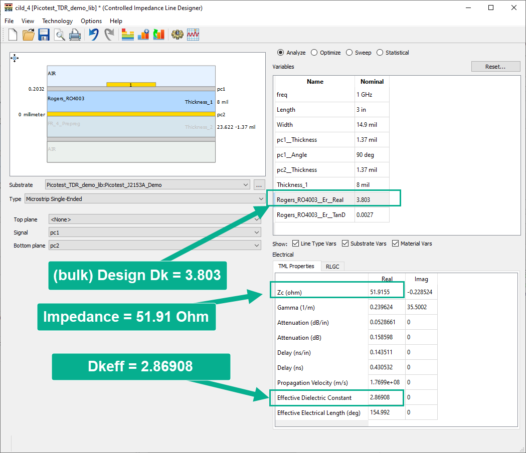
Fig. 5 - Keysight PathWave ADS Controlled Impedance Line Designer.
The Rogers online MWI calculator was used as a secondary check and the same parameters were entered as shown in Figure 6 [7]. The Rogers MWI calculator results in a Dkeff = 2.8255, within 1.5% of the 2.869 result from the PathWave ADS Controlled Impedance Line Designer.
As shown, our calculated results for the effective Dk using ADS and the MWI calculator are almost the same, so we have high confidence in the result. However, depending on the frequency of the signals traveling in your PCB design, these values may or may not provide enough assurance that your impedance will be tightly controlled. The reasoning behind this is that there is an absence of tolerance for design Dk since it depends on thickness, copper type or surface roughness, and PCB fabrication tolerances [8].
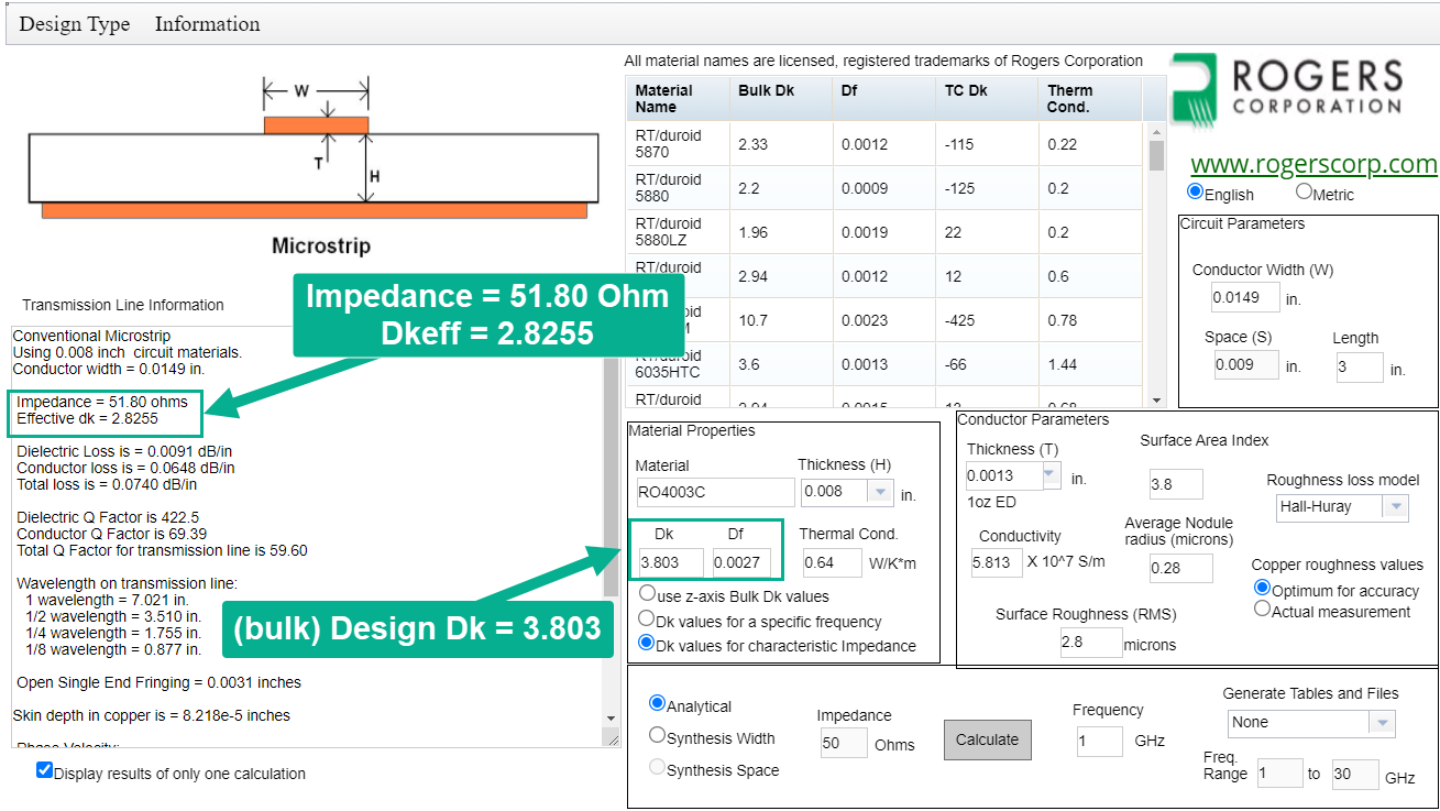
Fig. 6 - Rogers MWI Calculator Result for Picotest Demo Board.
Measurement of the Laminate’s Dkeff with a TDR
With the expected result for Dkeff defined, let’s measure the 3-inch trace on the TDR demo board for comparison with the simulated result.
For this measurement, we are using the Picotest J2154A TDR with a Tektronix MSO68B oscilloscope, and a Picotest P2105A, 16.5 GHz bandwidth, 40mil pitch TDR probe to contact the DUT.
Before we go further, let’s first discuss how to determine a TDR’s resolution limit. Per IPC-TM-650 2.5.5.7 [9], the TDR resolution limit is defined as a function of the total system rise time and the velocity of propagation.
 Where:
trsys = the TDR system rise time or fall time, 10% to 90%
Vp = the signal propagation velocity
In this measurement setup, the oscilloscope, probe, and TDR transition times affect the signal’s measured rise times and fall times. Therefore, the oscilloscope, probe, and TDR must be considered as a system to arrive at the true system rise time. In order to determine the total system rise time we can calculate the sum of squares as shown by EQ(8). 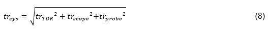
The rise time information for each component can be found in the respective datasheet. For the J2154A TDR, trTDR = 30ps. For the MSO68B, trscope = 40ps. For the P2105A (16.5 GHz) TDR probe, trProbe = 21.21 ps. Thus by EQ(8), trsys is

The resolution is relative to the pulse edge and the propagation speed. The propagation occurs at the effective Dk (Dkeff). Therefore with reference to EQ(2) and EQ(9), the resolution limit for the J2154A TDR, with MSO68B, using the P2105A TDR probe, with Dkeff = 2.82, which is from the MWI result shown in Figure 6, is calculated to be:
 This resolution limit tells us the minimum distance between structures that we can resolve as electrically long with enough fidelity using this TDR system. In other words, if the TDR system rise time is not fast enough, two discontinuities close together could overlap, making it difficult to differentiate between the structures on the transmission line [10]. Since the two copper trace markers on the demo board are placed exactly 3 inches (3000 mils) apart on the demo board trace, we know we have plenty of resolution using this TDR measurement setup.
Each of these copper markers appear capacitive, since they are wider than the signal trace. The result of each marker is an impedance dip. And since we know the exact separation of the markers, we can measure the round trip time between the impedance dips to obtain a precise signal travel time.
As shown by the setup in Figures 7 and 8 as well as the result captured in Figure 9, the round trip time measured, between the two markers, is measured and was found to be 883.066 ps. The Delta-time measurement accuracy (DTA) on the MSO68B is referenced from [11] to be 327.78 fs. That adds less than 0.04% total error to the measurement. In our measurement setup, the signal traces, math functions and cursor extractions are all averaged, greatly improving this accuracy. Without calibration, the tolerance of the 50 Ω port impedance is the dominant error. Measurement frequency, coupon length, and measurement locations are also defined by IPC-TM-650 2.5.5.7 [9].
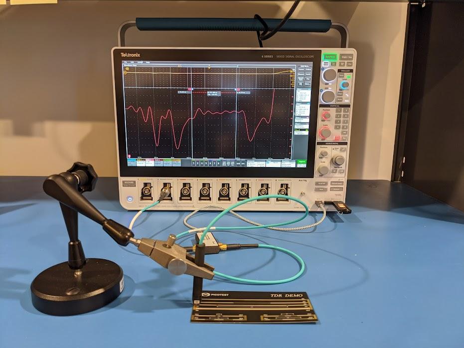
Fig. 7 - TDR Measurement Setup for the 3000 mil trace using the Picotest P2105A TDR Probe and J2154A Differential PerfectPulse® TDR with a Tektronix MSO68B oscilloscope.
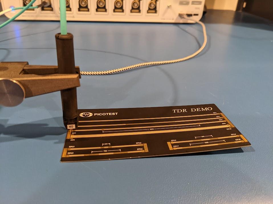
Fig. 8 - TDR Measurement Setup with the Demo Board TP5 Trace and the P2105A TDR Probe.
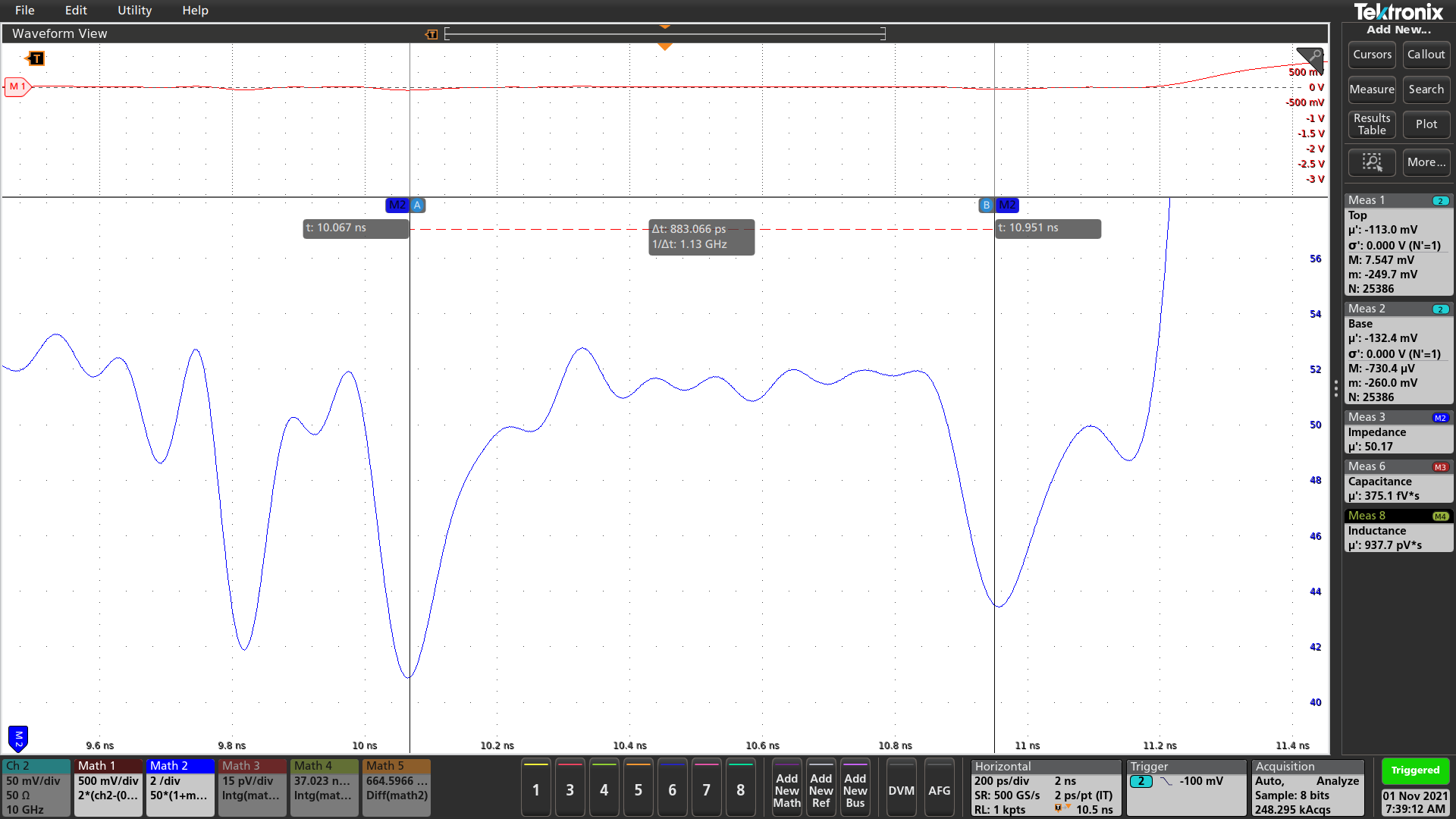
Fig. 9 - TDR Measurement of demo board TP5 Trace with the P2105A probe.
As shown by Figure 10, the average impedance of the TP5-TP6 trace is found by measuring the average impedance on the transmission between the 20% to 80% points to be 51.54Ω. The method used to calculate this impedance result has already been detailed [1]. However, it is important to note that this measurement setup uses math functions that include averaging on the signal traces and cursor extractions, which greatly improves the measurement signal-to-noise ratio (SNR) and therefore the effective number of bits (ENOB) and resolution.