
The power electronics engineer and the power integrity engineer share a common goal: provide the system with the correct voltages, currents, and noise characteristics to achieve the desired performance. Unfortunately, they do not share much else. They generally use different tools, vocabulary, and figures of merit. As a result, both sides lose.
A real system, as seen in Figure 1, includes a voltage regulator, the load circuitry and the printed circuit board (PCB), interconnects, and decoupling capacitors. The power electronics engineer is focused on performance at the power supply input and output terminals. The primary figures of merit are operating efficiency, size, weight, ripple, stability (typically assessed using the Bode plot), and load step response. Of course, there are other metrics, but this is a decent summary.
The power integrity engineer is focused on performance at the load circuit, which often means high-speed circuits (such as FPGAs, CPUs and data transceivers) as well as low-power devices (such as low noise amplifiers, sensors, and reference clocks). The primary figures of merit are noise, power rail impedance, and load induced transient response.
The power electronics engineer typically uses a SPICE simulator, while the power integrity engineer uses an electromagnetic simulator in order to account for PCB related parasitic effects.
The power electronic engineer refers to load regulation as the load current related voltage drop at the power supply, while the power integrity engineers refers to this as IR drop. A power electronic engineer refers to the voltage response to a load current change as step-load response or transient response while the power integrity engineer refers to this as ground bounce and VDD droop.
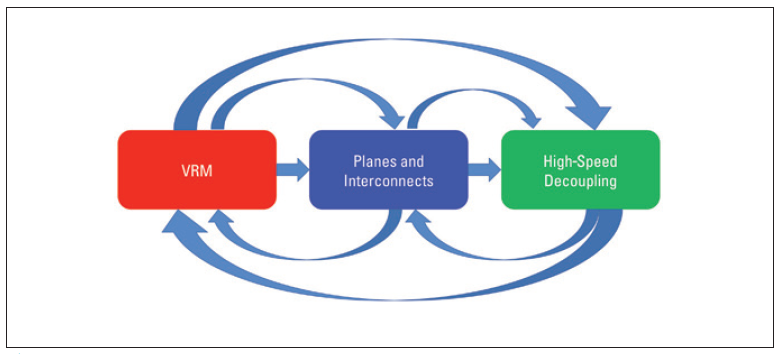
Figure 1. A typical system includes a voltage regulator, PCB and interconnects, and decoupling capacitors for the high-speed load. Both the voltage regulator and the load generate system noise. Impedance mismatches can amplify these noise sources.
Despite the fact that power electronics engineers and the power integrity engineers have different concerns, simulators, and vocabulary, they have impedance and noise concerns in common. For example, the PCB and decoupling capacitor impedance can negatively impact the stability of the voltage regulator, while the power supply and PCB impedance increase the load-induced transient voltage at the high-speed load. Unfortunately, both engineers are looking at the power of their device, and this is the wrong place!
The PCB is a transmission line, containing both inductance and capacitance. The voltage regulator impedance is typically much lower than the PCB characteristic impedance, resulting in a significant mismatch. The impedance mismatch results in resonant impedance peaks, further increasing the noise voltage at the high-speed load. Counterintuitively, the lower the VRM impedance is pushed, the higher the impedance is at the load. Raising the power supply impedance can improve the performance at the load. This effect is illustrated in Figure 2.
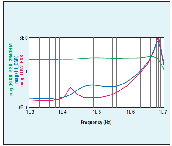
Figure 2. The impedance at a high-speed load is shown with three different power supply impedances. A low ESR ceramic capacitor (red trace) results in an 8Ω resonant peak at 7 MHz, while a higher ESR capacitor reduces this to 6Ω. Increasing the voltage regulator impedance to 2Ω eliminates the resonance and results in a much lower 2Ω peak impedance.
Figure 2 shows the impedance, as seen at the highspeed load, using three different voltage regulator source impedances. The three plots show the impact of a low ESR ceramic regulator output capacitor (red trace), a higher ESR tantalum output capacitor (blue trace), and a series resistor of 2Ω between the voltage regulator and the high-speed load. The 2Ω series resistor eliminates the 7 MHz resonance, and the maximum impedance is 2Ω. The higher ESR tantalum capacitor results in a higher impedance peak of 6Ω, while the low ESR ceramic capacitor results in the highest impedance peak of 8Ω.
This simple example clearly shows that impedance changes at the high-speed load can be opposite the impedance change at the power supply. For example, adding a low ESR capacitor at the voltage regulator to minimize spike noise can significantly increase the noise at the load.
In another example, we can cascade issues, resulting in incorrect design decisions. In Figure 3, the power supply switching frequency ripple is shown at both the power supply and at the high-speed load.

Figure 3. This simulation shows the power supply switching ripple at the power supply and also at the pins of the highspeed load. The EM simulator accounted for the PCB parasitics and decoupling capacitors. The power supply engineer and the power integrity engineer see different ripple. The power supply engineer might conclude (s)he needs to add more capacitors. This will add cost, size, weight, and reduce reliability. At the same time, the lower impedance will increase the impedance at the high-speed load, as shown previously. This incorrect interpretation results in a lose-lose outcome.
Due to the PCB parasitics and the decoupling capacitors, the ripple at the high-speed load is much smaller than at the VRM and has much less high-frequency content. The power supply engineer would look at the ripple at the power supply and decide to add much more filtering. This will add cost and weight, while reducing reliability and consuming valuable real estate on the PCB.
This design resolution will cascade, since adding capacitors at the voltage regulator will reduce the impedance at the voltage regulator output pins. As cited in the previous example, this will increase the noise at the high-speed load. The result of the added components, cost, reduced reliability, and real estate given to these filters is degraded performance, hence everyone loses. Of course, it is also possible that noise can be higher at the high-speed load than at the VRM as there are PCB resonances that align with noise frequencies corresponding to the voltage regulator noise voltage or harmonics of the noise voltage.
By establishing a flat power rail impedance magnitude and ripple noise tolerance, the power electronics engineer and the power integrity engineer can each focus mostly on their own terminals. The appropriate impedance is typically established using target impedance guidelines. A very rough estimate of the impedance is one third of the allowable voltage noise divided by the high-speed dynamic current, which should be available from the power integrity engineer. And, keep in mind that the power supply ripple will appear very differently at the high-speed load than it does at the power supply terminals.
When the system is completed and installed both engineers will achieve their desired goals. One more tip. If you are using an EM simulator, such as Keysight ADS, the voltage regulator, PCB with decoupling capacitor, and the high-speed load can all be simulated together.
Blog was published in the SIJ January 2019 Print Issue, Reflections: Page 14.